SLUS829G August 2008 – February 2020 UCC2897A
PRODUCTION DATA.
- 1 Features
- 2 Applications
- 3 Description
- 4 Revision History
- 5 Device Options
- 6 Pin Configuration and Functions
- 7 Specifications
-
8 Detailed Description
- 8.1 Overview
- 8.2 Functional Block Diagram
- 8.3 Feature Description
- 8.4 Device Functional Modes
- 9 Application and Implementation
- 10Power Supply Recommendations
- 11Layout
- 12Device and Documentation Support
- 13Mechanical, Packaging, and Orderable Information
封装选项
机械数据 (封装 | 引脚)
散热焊盘机械数据 (封装 | 引脚)
- RGP|20
订购信息
8.3.2 JFET Control and UVLO
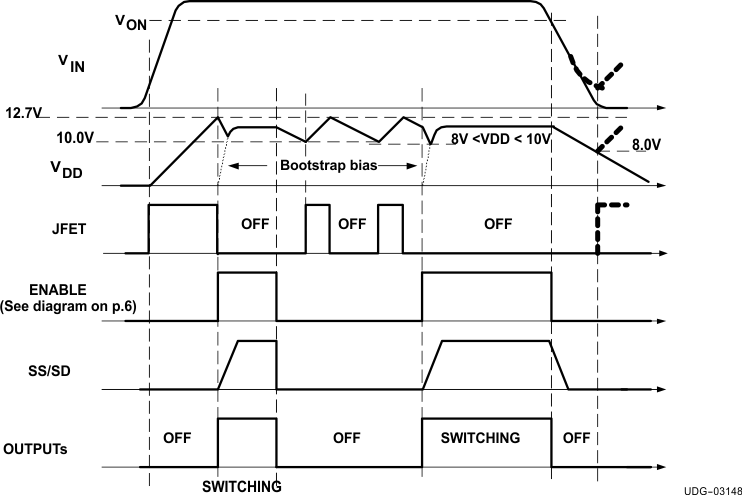
The UCC2897A controller includes a high-voltage JFET startup-transistor. The steady-state power-consumption of the of the control circuit which also includes the gate-drive power-loss of the two power switches of an active-clamp converter exceeds the current and thermal capabilities of the device. Thus the JFET should only be used for initial start-up of the control circuitry and to provide keep-alive power during stand-by mode when the gate-drive outputs are not switching. Accordingly, the startup device is managed by the control algorithm implemented on board the UCC2897A. The following timing diagram in Figure 19 illustrates the operation of the JFET startup device.

During initial power-up the JFET is on and charges the CBIAS and CHF capacitors connected to the VDD pin. The undervoltage lockout-circuit of the controller monitors the VDD pin to ensure proper biasing before the operation is enabled. When the VDD voltage reaches approximately 12.7 V (UVLO turnon threshold) the UVLO circuit enables the rest of the controller. At that time, the JFET turns off and 5 V appears on the VREF terminal. Switching waveforms might not appear at the gate-drive outputs unless all other conditions of proper operation are met. These conditions are:
- The voltage on the CS pin is below the current limit threshold
- The control voltage is above the zero duty-cycle boundary (VFB > 2.5 V).
- The input voltage is in the valid operating range (VVON < VVIN < VVOFF.
- The line under or overvoltage protections are not activated.
As the controller starts operation it draws bias power from the CBIAS capacitor until the bootstrap winding takes over (referring to Figure 25 and Figure 26). During this time, VDD voltage is falling rapidly as the JFET is off but the bootstrap voltage is still not sufficient to power the control circuits. It is imperative to store enough energy in CBIAS to prevent the bias voltage from dipping below the turnoff threshold of the UVLO circuit during the startup-time interval. Otherwise the power supply goes through several cycles of retry attempts before steady-state operation is established.
During normal operation the bias voltage is determined by the bootstrap bias design. The UCC2897A tolerates a wide range of bias voltages between the minimum-operating voltage (UVLO turn-off threshold) and the maximum-operating voltage as defined in the .
In applications where the power supply enters standby in response to an external command, the bias voltage of the controller must be kept alive to react intelligently to the control signal. In standby mode, switching action is suspended for an undefined period of time and the bootstrap power is unavailable to bias the controller. Without an alternate power source the bias voltage collapses and the controller initiates a re-start sequence. To avoid this situation, the onboard JFET of the UCC2897A controller keeps the VDD bias alive as long as the gate-drive outputs remain inactive. As shown in the timing diagram in Figure 19, the JFET turns on when VDD = 10 V and charges the CBIAS capacitor to approximately 12.7 V. At that time the JFET turns off and VDD gradually decreases to 10 V then the procedure repeats. When the power supply is enabled again, the controller is fully biased and ready to initiate the soft-start sequence. As soon as the gate-drive pulses appear the JFET turn off and bias is provided by the bootstrap bias generator.
During power down the situation is different as the switching action continues until the VDD bias voltage drops below the UVLO turn-off threshold of the controller (approximately 8 V). At that time the UCC2897A shuts down and turns off the 5-V bias rail and returning to startup state when the JFET device is turned on and the CBIAS capacitor starts charging again. In case the input voltage of the converter is re-established, the UCC2897A attempts to restart the converter.