SLUS829G August 2008 – February 2020 UCC2897A
PRODUCTION DATA.
- 1 Features
- 2 Applications
- 3 Description
- 4 Revision History
- 5 Device Options
- 6 Pin Configuration and Functions
- 7 Specifications
-
8 Detailed Description
- 8.1 Overview
- 8.2 Functional Block Diagram
- 8.3 Feature Description
- 8.4 Device Functional Modes
- 9 Application and Implementation
- 10Power Supply Recommendations
- 11Layout
- 12Device and Documentation Support
- 13Mechanical, Packaging, and Orderable Information
封装选项
机械数据 (封装 | 引脚)
散热焊盘机械数据 (封装 | 引脚)
- RGP|20
订购信息
6 Pin Configuration and Functions
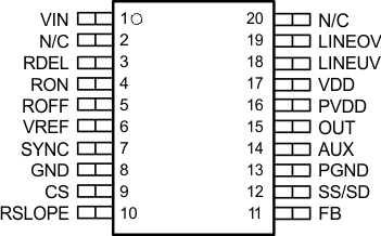
PW Package
20-Pin TSSOP
Top View

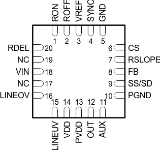
RGP Package
20-Pin VQFN
Bottom View

Pin Functions
| PIN | I/O | DESCRIPTION | ||
|---|---|---|---|---|
| NAME | NO. | |||
| TSSOP | VQFN | |||
| AUX | 14 | 11 | O | This output drives the auxiliary-clamp MOSFET which turns on when the main PWM-switching device turns off. The AUX pin directly drives the auxiliary switch with a 2-A source turn-on current and a 2-A sink turn-off current. |
| CS | 9 | 6 | I | This pin senses the peak current utilized for current-mode control and for current-limiting functions. The peak signal is applied to this pin before pulse-by-pulse current limiting activates and is approximately 0.5 V. |
| FB | 11 | 8 | I | This pin brings the error signal from an external optocoupler or error amplifier into the PWM-control circuitry. Often, there is a resistor tied from FB to VREF, and an optocoupler pulls the control pin closer to GND to reduce the pulse width of the OUT output driving the main-power switch of the converter. |
| GND | 8 | 5 | This pin serves as the fundamental-analog ground for the PWM-control circuitry. This pin is connected to PGND directly at the device. | |
| LINEOV | 19 | 16 | I | The LINEOV pin is an input pin of voltage comparator with programmable hysteresis and 1.27-V threshold, providing LINE overvoltage or other functions. |
| LINEUV | 18 | 15 | I | This pin provides a means to accurately enable/disable the power converter stage by monitoring the bulk input voltage or another parameter. When the circuit initially starts (or restarts from a disabled condition), a rising input on LINEUV enables the outputs when the threshold of 1.27 V is crossed. After the circuit is enabled, a falling LINEUV signal disables the outputs when the same threshold is reached. The hysteresis between the two levels is programmed using an internal current source. |
| OUT | 15 | 12 | O | This output pin drives the main PWM switching element MOSFET in an active-clamp controller. The OUT pin directly drives an N-channel device with a 2-A source turnon-current and a 2-A sink turnoff-current. TI recommends connecting a 10-kΩ resistor from this pin to PGND pin. |
| PGND | 13 | 10 | The PGND should serve as the current return for the high-current output drivers OUT and AUX. Ideally, the current path from the outputs to the switching devices, and back would be as short as possible, and enclose a minimal-loop area. | |
| PVDD | 16 | 13 | I | The PVDD pin is the supply pin for the power devices. It is separated internally from the VDD pin. |
| RSLOPE | 10 | 7 | I | A resistor connected from this pin to GND programs an internal current source that sets the slope-compensation ramp for the current-mode control-circuitry. |
| RTDEL | 3 | 20 | I | A resistor from this pin to GND programs the turn-on delay of the two gate-drive outputs to accommodate the resonant transitions of the active-clamp power converter. |
| ROFF | 5 | 2 | I | A resistor connected from this pin to GND programs an internal-current source that discharges the internal timing-capacitor. |
| RON | 4 | 1 | I | A resistor connected from this pin to GND programs an internal-current source that charges the internal timing-capacitor. |
| SS/SD | 12 | 9 | I | A capacitor from SS/SD to ground is charged by an internal-current source of IRON to program the soft-start interval for the controller. During a fault condition this capacitor is discharged by a current source equal to IRON. |
| SYNC | 7 | 4 | I | The SYNC pin serves as a bidirectional-synchronization input for the internal oscillator. The synchronization function is implemented such that the user-programmable maximum duty-cycle (set by RON and ROFF) remains accurate during synchronized operation. This pin is left open when not in use. The external capacitance is minimized. No capacitors are connected to this pin. |
| VDD | 17 | 14 | I | The VDD pin is the power supply for the device. There should be a 1-μF capacitor directly from VDD to PGND. The capacitor value should be at least 10-times larger than that on VREF. PGND and GND are connected externally and directly from PGND pin to GND pin. (To make a full design of capacitance on VDD pin, please refer to, Application Note: Understanding and Designing an Active Clamp Current Mode Controlled Converter (SLUA535), section 7.3) |
| VIN | 1 | 18 | I | This pin is connected to the input-power rail directly. Inside the device, a high-voltage start-up device is utilized to provide the start-up current for the controller until a bootstrap-type bias rail becomes available. |
| VREF | 6 | 3 | O | The VREF pin is the 5-V reference voltage that is used for an external load of up to 5 mA. Since this reference provides the supply rail for internal logic, VREF is bypassed to AGND as close as possible to the device. The VREF bias profile is not always monotonic before VDD reaches 5 V. |