ZHCSDI3A September 2014 – March 2015 UCC29950
PRODUCTION DATA.
- 1 特性
- 2 应用
- 3 说明
- 4 修订历史记录
- 5 Pin Configuration and Functions
- 6 Specifications
-
7 Detailed Description
- 7.1 Overview
- 7.2 Functional Block Diagram
- 7.3
Feature Description
- 7.3.1 Sense Networks
- 7.3.2 Sense Network Fault Detection
- 7.3.3 PFC Stage Soft-Start
- 7.3.4 AC Line Voltage Sensing
- 7.3.5 VBLK Sensing
- 7.3.6 AC Input UVLO and Brownout Protection
- 7.3.7 Dither
- 7.3.8 Active X-Cap Discharge
- 7.3.9 LLC Stage Soft Start
- 7.3.10 PFC Stage Current Sensing
- 7.3.11 Input Power Limit
- 7.3.12 PFC Stage Soft Start
- 7.3.13 Hybrid PFC Control Loop
- 7.3.14 PFC Stage Second Current Limit
- 7.3.15 PFC Inductor and Bulk Capacitor Recommendations
- 7.3.16 PFC Stage Over Voltage Protection
- 7.3.17 LLC Stage Control
- 7.3.18 Driver Output Stages and Characteristic
- 7.3.19 LLC Stage Dead Time Profile
- 7.3.20 LLC Stage Current Sensing
- 7.3.21 LLC Three Level Over-Current Protection
- 7.3.22 Over-Temperature Protection
- 7.3.23 Fault Timer and Control
- 7.4 Device Functional Modes
-
8 Application and Implementation
- 8.1 Application Information
- 8.2
Typical Application
- 8.2.1 Design Requirements
- 8.2.2
Detailed Design Procedure
- 8.2.2.1 LLC Stage
- 8.2.2.2 LLC Switching Frequency
- 8.2.2.3 LLC Transformer Turns Ratio
- 8.2.2.4 LLC Stage Equivalent Load Resistance
- 8.2.2.5 LLC Gain Range
- 8.2.2.6 Select LN and QE
- 8.2.2.7 LLC No-Load Gain
- 8.2.2.8 Parameters of the LLC Resonant Circuit
- 8.2.2.9 Verify the LLC Resonant Circuit Design
- 8.2.2.10 LLC Primary-Side Currents
- 8.2.2.11 LLC Secondary-Side Currents
- 8.2.2.12 LLC Transformer
- 8.2.2.13 LLC Resonant Inductor
- 8.2.2.14 Combining the LLC Resonant Inductor and Transformer
- 8.2.2.15 LLC Resonant Capacitor
- 8.2.2.16 LLC Stage with Split Resonant Capacitor
- 8.2.2.17 LLC Primary-Side MOSFETs
- 8.2.2.18 LLC Output Rectifier Diodes
- 8.2.2.19 LLC Stage Output Capacitors
- 8.2.2.20 LLC Stage Over-Current Protection, Current Sense Resistor
- 8.2.2.21 Detailed Design Procedure for the PFC stage
- 8.2.2.22 PFC Stage Output Current Calculation
- 8.2.2.23 Line Current Calculation
- 8.2.2.24 Bridge Rectifier
- 8.2.2.25 PFC Boost Inductor
- 8.2.2.26 PFC Input Capacitor
- 8.2.2.27 PFC Stage MOSFET
- 8.2.2.28 PFC Boost Diode
- 8.2.2.29 Bulk Capacitor
- 8.2.2.30 PFC Stage Current Sense Resistor
- 8.2.3 Application Curves
- 8.3 Do's and Don'ts
- 9 Power Supply Recommendations
- 10Layout
- 11器件和文档支持
- 12机械封装和可订购信息
8 Application and Implementation
8.1 Application Information
The UCC29950 device is a highly-integrated combo controller. It is designed for applications requiring a CCM boost PFC input stage followed by an LLC output / isolation stage. The PFC loop is internally compensated and requires no external loop-compensation components. EMI filtering is simplified because the PFC stage operates at a fixed frequency with dither. A three level output overload protection current/time profile is included.
8.2 Typical Application
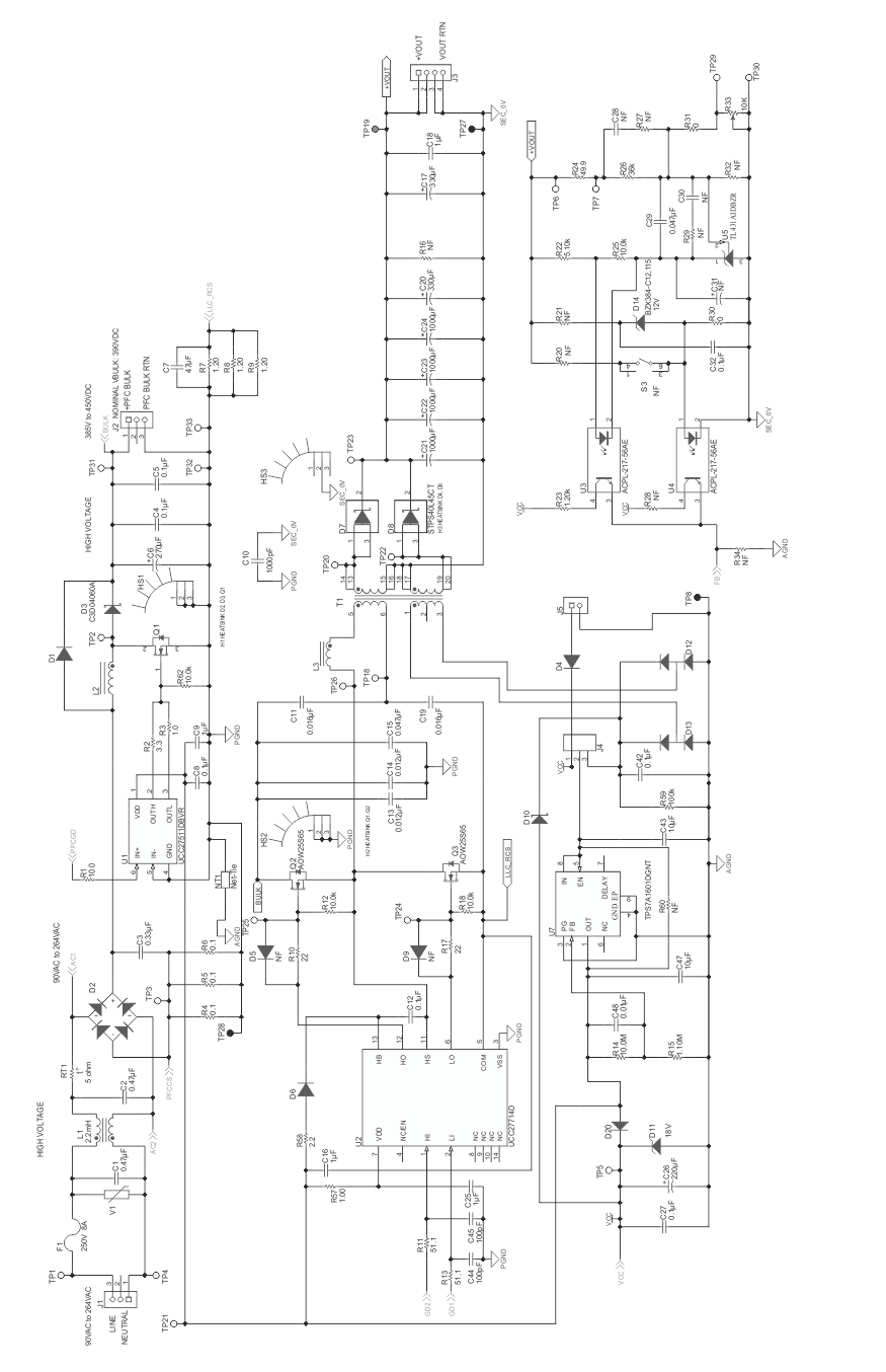
A typical application for this device would be in a 300-W, universal input isolated PSU with a 24-V (12.5-A) output.
8.2.1 Design Requirements
The typical application should meet the following requirements:
Table 5. Typical Application Requirements
| PARAMETER | REQUIREMENT | |
|---|---|---|
| VAC | Input voltage | 85 VAC to 264 VAC |
| fLINE | Line frequency | 47 Hz to 63 Hz |
| VBLK | Nominal PFC stage output voltage | 385 V |
| VBLK(ripple) | Max VBLK ripple (2 x Line Frequency) | 30 VPP |
| VBLK(max) | Maximum PFC stage output voltage, VBLK + ½ VBLK(ripple) | 400 V |
| VBLK(min) | Minimum PFC stage output voltage, VBLK – ½ VBLK(ripple) | 370 V |
| VBLK(hu) | Minimum PFC stage output voltage at end of hold-up time | 300 V |
| VOUT | Output voltage | 24 VDC |
| VOUT(min) | Min output voltage | 21.6 V (VOUT – 10%) |
| VOUT(max) | Max output voltage | 26.4 V (VOUT +10%) |
| IOUT | Full load output current | 12.5 A |
| VOUT(pk_pk) | Output voltage ripple | 300 mV |
| POUT | Output power | 300 W |
| η | Efficiency | 90 % |
| PF | Power factor | 0.99 |
| tH | Hold-up time | 20 ms |
| fPFC | PFC stage switching frequency | 98 kHz |
8.2.2 Detailed Design Procedure
8.2.2.1 LLC Stage
Start the design by deciding on the component values in the LLC power train and then move to the PFC stage.
The LLC stage design procedure outlined here follows the one given in the TI publication “Designing an LLC Resonant Half-Bridge Power Converter” which is available at http://www.ti.com/lit/ml/slup263/slup263.pdf. The document contains a full explanation of the origin of each of the equations used. The equations given below are based on the First Harmonic Approximation (FHA) method commonly used to analyze the LLC topology. This method gives a good starting point for any design, but a final design requires an iterative approach combining the FHA results, circuit simulation and hardware testing. An alternative design approach is given in (2) TI Application Note, LLC Design for UCC29950, Texas Instruments Literature Number SLUA733.
One of the reasons that the LLC topology is so popular is that it can achieve Zero Voltage Switching (ZVS) over a wide range of operating conditions. ZVS is important because it reduces switching losses in the power devices. The schematic for a basic LLC is shown in Figure 29.
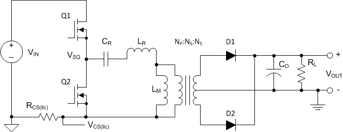 Figure 29. Basic LLC Schematic
In this system the input VIN is the output of the PFC stage. VIN is a DC voltage with some AC ripple at twice the line frequency. The two switches Q1 and Q2 are driven in anti-phase to generate a high-frequency square wave input signal VSQ at the input to the resonant network formed by CR, LR and LM. RCS(llc) is a current sensing resistor. Current flows in RCS(llc) only during the on time of Q1 in this single ended version of the LLC topology. This has two effects.
- There is a significant voltage ripple on the current sense signal as Q1 and Q2 are switched.
- Fault currents in Q2 are measured indirectly by their effect on currents in Q1.
The modified LLC topology shown in Figure 33 eliminates these disadvantages.
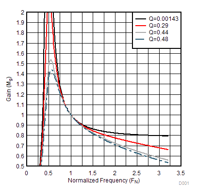
The resistor RL loads this circuit through the transformer turns ratio and the peak gain is therefore a function of load, as shown in Figure 30. At no load, RL is very high and its influence may be neglected and circuit has a resonance at:
At the other extreme, RL is zero and it effectively shorts the transformer magnetizing inductance LM. The resonant frequency under this condition is:

This means that as the load changes from no load to short circuit the peak-gain frequency (fC0) moves between these two values so that:

Output voltage regulation is achieved by changing the switching frequency of the LLC stage. If VIN increases the LLC stage gain must reduce in order to keep VOUT unchanged. The gain is reduced by increasing the switching frequency as can be seen in Figure 30. If VIN reduces, then the gain must be increased and this is done by reducing the switching frequency. The frequency must remain above the resonant frequency fC0 to maintain zero voltage switching and to avoid control law reversal. This is especially important in a short circuit condition where the control loop would try to reduce the switching frequency and where simultaneously fC0 has increased to its maximum at f0. Short circuit and overload protection are provided in the UCC29950 and are discussed in LLC Stage Over-Current Protection, Current Sense Resistor below.
8.2.2.2 LLC Switching Frequency
Selecting the nominal full-load switching frequency is relatively straightforward. Most EMI standards for conducted emissions have a lower limit at 150 kHz. If the fundamental switching frequency is lower than this then it does not appear in the EMI test scans which makes EMI filtering easier. Otherwise, if it is too low then the magnetic components are larger than necessary and the efficiency benefits of ZVS are reduced. A switching frequency of 120 kHz is a good compromise and is the one used in this design.
8.2.2.3 LLC Transformer Turns Ratio
The transformer turns ratio is given by the equation:

VIN is the voltage on the bulk capacitor. This is regulated at 385 VDC if the resistor values suggested in Table 2 are used for the potential divider at the VBULK pin and ignoring diode forward voltage drops VOUT is 24 V.
8.2.2.4 LLC Stage Equivalent Load Resistance
This is the effective load resistance reflected through the transformer turns ratio. Re is determined at the full load point.

8.2.2.5 LLC Gain Range
These parameters set the gain range required of the LLC stage. It is assumed a 0.5-V drop in the rectifier diodes (Vf) and a further 0.5-V drop due to other losses (VLOSS).


8.2.2.6 Select LN and QE
From Figure 31 and Figure 32select suitable LN and QE values to meet the MG_MIN and MG_MAX values from Equation 8 and Equation 9.
LN is the primary inductance ratio and is given by:

QE is the quality factor of the resonant network.

Set LN = 5.0 and QE = 0.40 for this application. The LLC peak gain curves below show a maximum which is greater than the maximum calculated by Equation 9.
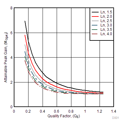 Figure 31. LLC Peak Gain Curves
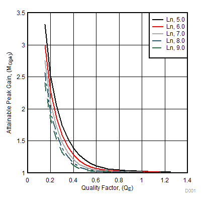 Figure 32. LLC Peak Gain Curves
8.2.2.7 LLC No-Load Gain
The gain required at no load is:

Figure 30 shows that the design can achieve a minimum gain of 0.8 at the maximum frequency of the UCC29950 (350 kHz or 2.9 times the normalized f0 of 120 kHz).). If the gain is too high then the UCC29950 enters a burst mode of operation to keep the output voltage under control.
8.2.2.8 Parameters of the LLC Resonant Circuit
The value of the resonant capacitor is given by the equation:

The resonant inductor is given by the equation:

Rearranging Equation 10gives a value for LM, the transformer magnetizing inductance:

8.2.2.9 Verify the LLC Resonant Circuit Design
The series resonant frequency is given by Equation 4.

The inductance ratio is given by:
The quality factor at full load is given by:

This differs from the initial value of 0.45 because a rounded value for CR is used here and in the calculation of LR.
The difference is not significant.
Figure 30 has been normalized to the series resonant frequency which is 120 kHz in this example.
At the minimum gain condition with minimum output voltage and maximum input voltage (MG(min)) the frequency is 1.6 times f0 or fSW(max) = 192 kHz.
At the maximum gain condition with maximum output voltage and minimum input voltage (MG(max)) the frequency is 0.6 times f0 or fSW(min) = 72 kHz.
8.2.2.10 LLC Primary-Side Currents
The primary-side RMS load current is given by:

The RMS magnetizing current at minimum switching frequency is:

The total current in the resonant circuit is then given by:

This current also flows in the transformer primary winding (IWP) and the resonant capacitor (ICR).
8.2.2.11 LLC Secondary-Side Currents
The total secondary-side RMS current is the current referred from the primary side (IOE) to the secondary side.

The design uses a centre tapped secondary so that this current is shared equally between the two windings. The current in each winding is then:

And the half-wave average current in the secondary windings is:

8.2.2.12 LLC Transformer
The transformer can be built or purchased according to these specifications:
- Turns Ratio (N): 8
- Primary Magnetizing Inductance: LM = 275 µH
- Primary Terminal Voltage: 450 VAC
- Primary Winding Rated Current: IWP = 2.4 A
- Secondary Terminal Voltage: 56 VAC
- Secondary Winding Rated Current: IWS = 10.8 A
- No Load Operating Frequency: fSW(max) = 192 kHz
- Full Load Operating Frequency: fSW(min) = 72 kHz
- Reinforced Insulation Barrier from Primary-to-Secondary to IEC60950
The minimum operating frequency during normal operation is that calculated above but during shutdown the LLC can operate at at LLCFMIN .The magnetic components in the resonant circuit, the transformer and resonant inductor, should be rated to operate at this lower frequency.
8.2.2.13 LLC Resonant Inductor
The AC voltage across the resonant inductor is given by its impedance times the current:

As with the transformer, the resonant inductor can be built or specified according to these specifications:
- Inductance: LR = 55 µH
- Rated Current: IR = 2.4 A
- Terminal AC Voltage: VLR = 60 V
- Frequency Range: 72 kHz to 192 kHz.
The minimum operating frequency during normal operation is that calculated above but during shutdown the LLC can operate at at LLCFMIN.The magnetic components in the resonant circuit, the transformer and resonant inductor, should be rated to operate at this lower frequency.
8.2.2.14 Combining the LLC Resonant Inductor and Transformer
All physical transformers have a certain amount of leakage inductance. This inductance appears in series with the magnetizing inductance. It degrades the performance of most topologies so designers usually try to minimize it. In the LLC topology however, the leakage inductance appears in the same position as the Resonant Inductor LR in Figure 29. This means that it is possible to design the transformer so that its leakage inductance replaces the separate resonant inductor.
- Fewer Magnetic Components
- Simpler PCB
- Lower Cost
The Advantages:
The disadvantage to the transformer must be designed to have a relatively large and well controlled amount of leakage inductance. The resonant inductance in the design above is about 20% of the total LR + LM. This is a high ratio and careful control of the winding geometry and layering is needed to keep the leakage inductance within acceptable limits.
The design procedure given above is valid irrespective of whether a design uses a separate resonant inductor and transformer or uses a single high-leakage transformer.
8.2.2.15 LLC Resonant Capacitor
This capacitor carries the full-primary current at a high frequency. A low dissipation factor part is needed to prevent overheating in the part.
The AC voltage across the resonant capacitor is given by its impedance times the current.


And the corresponding peak voltage:
The part selected must meet these specifications:
- Rated Current: ICR = 2.4 A
- AC Voltage: VCR(peak) = 434 V
8.2.2.16 LLC Stage with Split Resonant Capacitor
It is possible to split the resonant capacitor in Figure 29 into two separate parts as shown below. The two circuits are topologically equivalent but there are some differences in circuit stresses. The calculation of the resonant circuit components is the same and the values of LR, LM and CR are unchanged. The two resonant capacitors are each half the value of CR.
The major advantages are:
- The current stresses in the capacitors are halved because the resonant current is shared between the two parts.
- The currents during the conduction times of both Q1 and Q2 flow in the current sensing resistor.
The main disadvantage is two parts are needed.
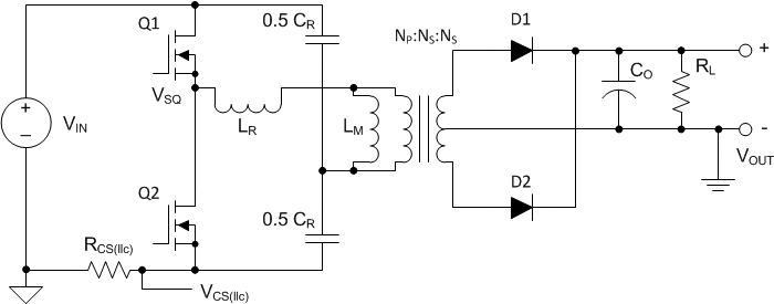 Figure 33. Basic LLC Schematic with Split Resonant Capacitor
8.2.2.17 LLC Primary-Side MOSFETs
VIN appears across the MOSFET which is not conducting. The voltage rating must then be:

This is a minimum rating and a 650-V rated part would be a better choice to allow margin for line-surge tests.
In the steady state, each MOSFET carries half of the resonant current. Start-up currents can be significantly higher so we set the RMS current rating to 110 % of the resonant current.

8.2.2.18 LLC Output Rectifier Diodes
The voltage rating for the output diodes is given by:

The current rating for the output diodes is given by:

8.2.2.19 LLC Stage Output Capacitors
The LLC converter topology does not require an output filter although a small second stage filter inductor may be useful in reducing peak-to-peak output noise.
Assuming that the output capacitors carry the rectifier’s full wave output current then the capacitor ripple current rating is:

The capacitor’s RMS current rating at 120 kHz is:

Solid Aluminum capacitors with conductive polymer technology have high ripple-current ratings and are a good choice here. The ripple-current rating for a single capacitor may not be sufficient so multiple capacitors are often connected in parallel.
The ripple voltage at the output of the LLC stage is a function of the amount of AC current that flows in the capacitors. To estimate this voltage, we assume that all the current, including the DC current in the load, flows in the filter capacitors.

The capacitor specifications are:
- Voltage Rating: 30 V
- Ripple Current Rating: 6.04 A at 120 kHz
- ESR: < 15 mΩ
8.2.2.20 LLC Stage Over-Current Protection, Current Sense Resistor
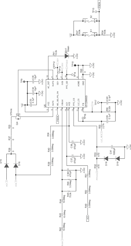
This resistor shown in Figure 29 and Figure 33 senses the LLC stage input current. This current contains a significant component at the switching frequency in additional to a DC component. Only the DC component is proportional to the load current. This means that the signal should be filtered before it is applied to the LLC_CS pin of the UCC29950. The degree of filtering is a compromise between response time and accuracy. A recommended schematic is shown in Figure 13. An RC filter with a pole at about 1 kHz is used to filter the signal. An additional capacitor, C1, across the current sense resistor provides a higher frequency pole at approximately 10 kHz.
The LLC current sensing resistor is selected so that the LLC_CS signal is at 90% of the OCP1 level (400 mV x 0.9 = 360 mV) when the converter is operating at full load and nominal input and output conditions. The resistor value is then given by:
Where VBLK(min) is the voltage at the bottom of the line ripple on CBLK.
Assuming there is no ripple current in the current sensing resistor, the full load power dissipated in this resistor is given by:
The resistor should be able to dissipate the power due to an overload which is just lower than the OCP_1 threshold.
8.2.2.21 Detailed Design Procedure for the PFC stage
The boost topology operated in Continuous Conduction Mode (CCM) is a popular choice for a Power Factor Correction (PFC) stage because it has lower component stresses than other topologies. This becomes more important at higher power levels.
The schematic for a basic PFC is shown in Figure 34. The basic schematics for the three boost PFC circuits, Discontinuous Conduction Mode (DCM), Transition Mode (TM) and CCM, are the same. The differences relate to whether or not the inductor current is allowed to go to zero for part of the PWM cycle (DCM) and whether the PFC frequency is held constant or used as a control variable (TM)
 Figure 34. Basic PFC Schematic
8.2.2.22 PFC Stage Output Current Calculation
The first step is to determine the maximum load current on the PFC stage, allowing for an overload to 110 % of maximum load power.

8.2.2.23 Line Current Calculation
Next determine the maximum RMS input-line current, allowing for an overload to 110% of maximum load power.

The peak line current is:

The average line current is given by:

8.2.2.24 Bridge Rectifier
A typical bridge rectifier has a forward voltage drop VF_BR of 0.95 V. The power loss in the bridge rectifier can be calculated from:

The bridge rectifier must be rated to carry the full-line current (ILINE(avg_max)). The voltage rating of the bridge should be at least 600 V. The bridge rectifier also carries the full inrush current as the bulk capacitor (CBLK) charges when the line is connected. The amplitude and duration of this current is difficult to determine in advance because it depends on many unknown parameters.
8.2.2.25 PFC Boost Inductor
The boost inductor is usually chosen so that the peak-to-peak amplitude of the switching frequency ripple current, IHFR(pfc), is between 20% and 40% of the average current at peak of line. This design example uses IHFR_PFC = 30%. Numerically this is, (from Equation 41)

The minimum boost inductor value is calculated from a worst case duty cycle of 50%.

The boost inductor must be able to support a maximum current of:

The boost inductor specifications are:
- LPFC = 550 µH
- Current = 7 A
8.2.2.26 PFC Input Capacitor
The purpose of the input capacitor is to provide a local, low-impedance source for the high-frequency ripple currents which flow in the PFC inductor. The allowed voltage ripple on CIN is ΔVIN.


An X2 film capacitor is normally chosen for this application.
8.2.2.27 PFC Stage MOSFET
The main specifications for the PFC stage MOSFET are:
- BVDSS, Drain Source Breakdown Voltage, ≥ 650 V
- RDS(on), On State Drain Source Resistance, 460 mΩ (125 °C)
- COSS, Output Capacitance, 87 pF
- tr, device rise time, 30 ns
- tf device fall time, 34 ns
The losses in the device are calculated below. These calculations are approximations because the losses are dependent on parameters which are not well controlled. For example the RDS(on) of a MOSFET can vary by a factor of 2 from 25°C to 125°C. Therefore several iterations may be needed to choose an optimum device for an application different to the one discussed.
The conduction losses are estimated by:

Numerically:

The switching losses in the MOSFET are estimated by:

Numerically:


8.2.2.28 PFC Boost Diode
Reverse recovery losses can be significant in a CCM boost converter so a silicon carbide diode is chosen here because it has no reverse recovery charge, QRR, and therefore zero reverse recovery losses. The disadvantage is that the cost is higher than that of Silicon ultra fast diodes. The losses are estimated as follows:

8.2.2.29 Bulk Capacitor
The value of the bulk capacitor is determined by three factors.
- To ensure loop stability, the capacitance must be between 0.5 μF W-1 and 2.4 μF W-1 (see PFC Inductor and Bulk Capacitor Recommendations). For this 300-W application a bulk capacitance in the range 150 μF to 720 μF is allowed.
- It must be large enough to provide the required hold-up time.
- It must be large enough to keep the ripple at twice line frequency within the required limits.
The UCC29950 continues to run the LLC stage until the voltage at the VBULK pin has fallen below VBULK(llc_stop) (0.49 V). This corresponds to a VBLK of 200 V if the specified values for RBOT and RTOP are used. From Equation 55 it can be see that the LLC stage will not have enough gain to maintain VOUT with such a low input voltage. The minimum voltage at which the LLC stage regulates is determined from Equation 55 which is a rearrangement of Equation 10. MG(max) is found from Figure 31 which gives a maximum gain of the LLC stage of 1.33.
The value of the capacitor is then given by:

270 µF for 300 W is equal to 0.9 µF W-1 which lies within the allowed range for loop stability.
The peak-to-peak ripple voltage at twice line frequency on CBLK is calculated as follows:

The result of this calculation, 11.3 V, is significantly better than the specification, 30 V. This is because the size of the bulk capacitor is determined by the hold-up time rather than by the peak-to-peak line ripple specification.
The ripple current flowing in the bulk capacitor depends on the duty cycle which varies over the line cycle and also as a function of the RMS value of the line voltage. This makes a precise calculation difficult however Equation 58 gives a good approximation.

8.3 Do's and Don'ts
Don’t probe the SUFG pin unless absolutely necessary. A normal X10 Oscilloscope probe can significantly load the very high output impedance of this pin .
Pay careful attention to grounding and to the routing of the sensing signals at PFC_CS, LLC_CS, VBULK, AC1 and AC2 pins.
The UCC29950 uses low value PFC current sense resistors, 38 mΩ in the example above. Careful attention to layout is needed to avoid significant errors in the PFC current and power limit points. Use Kelvin connections to the resistors.
