ZHCSIU2K June 2001 – November 2023 UCC27323 , UCC27324 , UCC27325 , UCC37323 , UCC37324 , UCC37325
PRODUCTION DATA
- 1
- 1 特性
- 2 应用
- 3 说明
- 4 Device Comparison Table
- 5 Pin Configuration and Functions
- 6 Specifications
- 7 Detailed Description
- 8 Application and Implementation
- 9 Power Supply Recommendations
- 10Layout
- 11Device and Documentation Support
- 12Revision History
- 13Mechanical, Packaging, and Orderable Information
封装选项
机械数据 (封装 | 引脚)
散热焊盘机械数据 (封装 | 引脚)
- DGN|8
订购信息
8.2.3 Application Curves
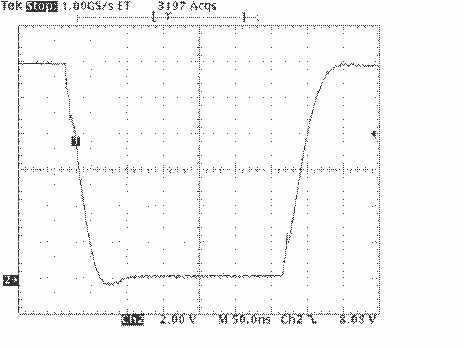
Figure 8-5 shows the circuit performance achievable with a single driver (half of the 8-pin IC) driving a 10-nF load. The input pulse width (not shown) is set to 300 ns to show both transitions in the output waveform. Note the linear rise and fall edges of the switching waveforms which is due to the constant output current characteristic of the driver as opposed to the resistive output impedance of traditional MOSFET-based gate drivers.
Sink and source currents of the driver are dependent upon the VDD value and the output capacitive load. The larger the VDD value, the higher the current capability; also, the larger the capacitive load, the higher the current sink and source capability.
Trace resistance and inductance, including wires and cables for testing, slows down the rise and fall times of the outputs; thus reducing the current capabilities of the driver.
To achieve higher current results, reduce resistance and inductance on the board as much as possible and increase the capacitive load value in order to swamp out the effect of inductance values.

| CL = 10 nF, CL = 10 nF, VDD = 12 V |