SLUS270G March   1999  – May 2020 UCC2800 , UCC2801 , UCC2802 , UCC2803 , UCC2804 , UCC2805

PRODUCTION DATA  

  1. Features
  2. Applications
  3. Description
  4. Revision History
  5. Description (continued)
  6. Device Comparison Table
  7. Pin Configuration and Functions
    1.     Pin Functions
  8. Specifications
    1. 8.1 Absolute Maximum Ratings
    2. 8.2 ESD Ratings
    3. 8.3 Recommended Operating Conditions
    4. 8.4 Thermal Information
    5. 8.5 Electrical Characteristics
    6. 8.6 Typical Characteristics
  9. Detailed Description
    1. 9.1 Overview
    2. 9.2 Functional Block Diagram
    3. 9.3 Feature Description
      1. 9.3.1  Detailed Pin Description
        1. 9.3.1.1 COMP
        2. 9.3.1.2 FB
        3. 9.3.1.3 CS
        4. 9.3.1.4 RC
        5. 9.3.1.5 GND
        6. 9.3.1.6 OUT
        7. 9.3.1.7 VCC
        8. 9.3.1.8 Pin 8 (REF)
      2. 9.3.2  Undervoltage Lockout (UVLO)
      3. 9.3.3  Self-Biasing, Active Low Output
      4. 9.3.4  Reference Voltage
      5. 9.3.5  Oscillator
      6. 9.3.6  Synchronization
      7. 9.3.7  PWM Generator
      8. 9.3.8  Minimum Off-Time Setting (Dead-Time Control)
      9. 9.3.9  Leading Edge Blanking
      10. 9.3.10 Minimum Pulse Width
      11. 9.3.11 Current Limiting
      12. 9.3.12 Overcurrent Protection and Full Cycle Restart
      13. 9.3.13 Soft Start
      14. 9.3.14 Slope Compensation
    4. 9.4 Device Functional Modes
      1. 9.4.1 Normal Operation
      2. 9.4.2 UVLO Mode
      3. 9.4.3 Soft Start Mode
      4. 9.4.4 Fault Mode
  10. 10Application and Implementation
    1. 10.1 Application Information
    2. 10.2 Typical Application
      1. 10.2.1 Design Requirements
      2. 10.2.2 Detailed Design Procedure
        1. 10.2.2.1 Current Sensing Network
        2. 10.2.2.2 Gate Drive Resistor
        3. 10.2.2.3 Vref Capacitor
        4. 10.2.2.4 RTCT
        5. 10.2.2.5 Start-Up Circuit
        6. 10.2.2.6 Voltage Feedback Compensation
          1. 10.2.2.6.1 Power Stage Gain, Zeroes, and Poles
          2. 10.2.2.6.2 Compensation Loop
      3. 10.2.3 Application Curves
  11. 11Power Supply Recommendations
  12. 12Layout
    1. 12.1 Layout Guidelines
    2. 12.2 Layout Example
  13. 13Device and Documentation Support
    1. 13.1 Support Resources
    2. 13.2 Trademarks
    3. 13.3 Electrostatic Discharge Caution
    4. 13.4 Glossary
    5. 13.5 Related Links
  14. 14Mechanical, Packaging, and Orderable Information

封装选项

机械数据 (封装 | 引脚)
散热焊盘机械数据 (封装 | 引脚)
订购信息

Typical Application

Figure 10-1 illustrates a typical circuit diagram for an AC-DC converter using the UCC2800 in a peak current mode controlled flyback application.
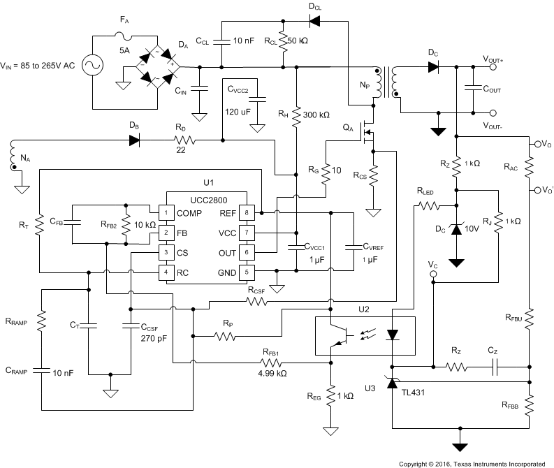
GUID-4E1BDB6D-17C9-4A80-8722-FFE9358ABA2D-low.gifFigure 10-1 Typical Application Circuit