SLUS168E Apr 1999 – August 2015 UCC2808-1 , UCC2808-2 , UCC3808-1 , UCC3808-2
PRODUCTION DATA.
6 Specifications
6.1 Absolute Maximum Ratings
over operating free-air temperature range (unless otherwise noted)(1)| MIN | MAX | UNIT | ||
|---|---|---|---|---|
| Supply voltage (IDD ≤ 10 mA) | 15 | V | ||
| Supply current | 20 | mA | ||
| OUTA/OUTB source current (peak)(2) | –0.5 | A | ||
| OUTA/OUTB sink current (peak)(2) | 1.0 | A | ||
| Analog inputs (FB, CS) – 0.3 V to VDD+0.3 V | 6 | V | ||
| Power dissipation at TA = 25 ° C (N Package) | 1 | W | ||
| Power dissipation at T A = 25 ° C (D Package) | 650 | mW | ||
| Power dissipation at T A = 25 ° C (PW Package) | 400 | mW | ||
| TJ | Junction temperature | –55 | 150 | °C |
| Lead temperature (soldering, 10 sec.) | 300 | °C | ||
| Tstg | Storage temperature | –65 | 150 | °C |
(1) Stresses beyond those listed under Absolute Maximum Ratings may cause permanent damage to the device. These are stress ratings only, which do not imply functional operation of the device at these or any other conditions beyond those indicated under Recommended Operating Conditions. Exposure to absolute-maximum-rated conditions for extended periods may affect device reliability.
(2) Currents are positive into, negative out of the specified terminal. Consult Packaging Section of the Power Supply Control Data Book (SLUD003) for thermal limitations and considerations of packages.
6.2 ESD Ratings
| VALUE | UNIT | |||
|---|---|---|---|---|
| V(ESD) | Electrostatic discharge | Human body model (HBM), per ANSI/ESDA/JEDEC JS-001(1) | ±2500 | V |
| Charged-device model (CDM), per JEDEC specification JESD22-C101(2) | ±1500 | |||
(1) JEDEC document JEP155 states that 500-V HBM allows safe manufacturing with a standard ESD control process.
(2) JEDEC document JEP157 states that 250-V CDM allows safe manufacturing with a standard ESD control process.
6.3 Recommended Operating Conditions
over operating free-air temperature range (unless otherwise noted)| MIN | MAX | UNIT | |||
|---|---|---|---|---|---|
| VDD | Supply Voltage | UCCx808-1 | 13 | 14 | V |
| UCCx808-2 | 5 | 14 | |||
| TJ | Junction Temperature | UCC2808-x | –40 | 85 | °C |
| UCC3808-x | 0 | 70 | |||
6.4 Electrical Characteristics
TA = 0°C to 70°C for the UCC3808-x, –40°C to 85°C for the UCC2808-x and –55°C to 125°C for the UCC1808-x, VDD = 10 V(6), 1-μF capacitor from VDD to GND, R = 22 kΩ , C = 330 pF, TA = TJ , (unless otherwise specified)| PARAMETER | TEST CONDITIONS | MIN | TYP | MAX | UNIT | |
|---|---|---|---|---|---|---|
| OSCILLATOR SECTION | ||||||
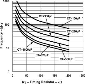
| Oscillator frequency | 175 | 194 | 213 | kHz | ||
| Oscillator amplitude/VDD(1) | 0.44 | 0.5 | 0.56 | V/V | ||
| ERROR AMPLIFIER SECTION | ||||||
| Input voltage | COMP = 2 V | 1.95 | 2 | 2.05 | V | |
| Input bias current | –1 | 1 | μ A | |||
| Open-loop voltage gain | 60 | 80 | dB | |||
| COMP sink current | FB = 2.2 V, COMP = 1 V | 0.3 | 2.5 | mA | ||
| COMP source current | FB = 1.3 V, COMP = 3.5 V | –0.25 | –0.5 | mA | ||
| PWM SECTION | ||||||
| Maximum duty cycle | Measured at OUTA or OUTB | 48% | 49% | 50% | ||
| Minimum duty cycle | COMP = 0 V | 0% | ||||
| CURRENT SENSE SECTION | ||||||
| Gain(2) | 1.9 | 2.2 | 2.5 | V/V | ||
| Maximum input signal | COMP = 5 V (3) | 0.45 | 0.5 | 0.55 | V | |
| CS to output delay | COMP = 3.5 V, CS from 0 to 600 mV | 100 | 200 | ns | ||
| CS source current | –200 | nA | ||||
| Over current threshold | 0.7 | 0.75 | 0.8 | V | ||
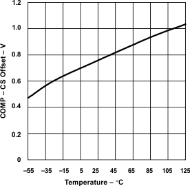
| COMP to CS offset | CS = 0 V | 0.35 | 0.8 | 1.2 | V | |
| OUTPUT SECTION | ||||||
| OUT low level | I = 100 mA | 0.5 | 1 | V | ||
| OUT high level | I = – 50 mA, VDD – OUT | 0.5 | 1 | V | ||
| Rise time | CL = 1 nF | 25 | 60 | ns | ||
| Fall time | CL = 1 nF | 25 | 60 | ns | ||
| UNDERVOLTAGE LOCKOUT SECTION | ||||||
| Start threshold | UCCx808-1 (6) | 11.5 | 12.5 | 13.5 | V | |
| UCCx808-2 | 4.1 | 4.3 | 4.5 | |||
| Minimum operating voltage after start | UCCx808-1 | 7.6 | 8.3 | 9 | V | |
| UCCx808-2 | 3.9 | 4.1 | 4.3 | |||
| Hysteresis | UCCx808-1 | 3.5 | 4.2 | 5.1 | V | |
| UCCx808-2 | 0.1 | 0.2 | 0.3 | |||
| SOFT-START SECTION | ||||||
| COMP rise time | FB = 1.8 V, rise from 0.5 V to 4 V | 3.5 | 20 | ms | ||
| OVERALL SECTION | ||||||
| Start-up current | VDD < start threshold | 130 | 260 | µA | ||
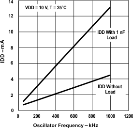
| Operating supply current | FB = 0 V, CS = 0 V (5)(6) | 1 | 2 | mA | ||
| VDD zener shunt voltage | IDD = 10 mA (4) | 13 | 14 | 15 | V | |
(1) Measured at RC. Signal amplitude tracks VDD.
(2) Gain is defined by:  0 v VCS v 0.4 V
 0 v VCS v 0.4 V
 (3) Parameter measured at trip point of latch with FB at 0 V.
(4) Start threshold and Zener shunt threshold track one another.
(5) For UCCx808 – 1, set VDD above the start threshold before setting at 10 V
(6) Does not include current in the external oscillator network.
6.5 Typical Characteristics


