SLUS161F April 1999 – May 2020 UCC2813-0 , UCC2813-1 , UCC2813-2 , UCC2813-3 , UCC2813-4 , UCC2813-5 , UCC3813-0 , UCC3813-1 , UCC3813-2 , UCC3813-3 , UCC3813-4 , UCC3813-5
PRODUCTION DATA.
- 1 Features
- 2 Applications
- 3 Description
- 4 Revision History
- 5 Device Comparison Table
- 6 Pin Configuration and Functions
- 7 Specifications
-
8 Detailed Description
- 8.1 Overview
- 8.2 Functional Block Diagram
- 8.3
Feature Description
- 8.3.1 Detailed Pin Descriptions
- 8.3.2 Undervoltage Lockout (UVLO)
- 8.3.3 Self-Biasing, Active Low Output
- 8.3.4 Reference Voltage
- 8.3.5 Oscillator
- 8.3.6 Synchronization
- 8.3.7 PWM Generator
- 8.3.8 Minimum Off-Time Adjustment (Dead-Time Control)
- 8.3.9 Leading Edge Blanking
- 8.3.10 Minimum Pulse Width
- 8.3.11 Current Limiting
- 8.3.12 Overcurrent Protection and Full-Cycle Restart
- 8.3.13 Soft Start
- 8.3.14 Slope Compensation
- 8.4 Device Functional Modes
-
9 Application and Implementation
- 9.1 Application Information
- 9.2
Typical Application
- 9.2.1 Design Requirements
- 9.2.2
Detailed Design Procedure
- 9.2.2.1 Bulk Capacitor Calculation
- 9.2.2.2 Transformer Design
- 9.2.2.3 MOSFET and Output Diode Selection
- 9.2.2.4 Output Capacitor Calculation
- 9.2.2.5 Current Sensing Network
- 9.2.2.6 Gate Drive Resistor
- 9.2.2.7 REF Bypass Capacitor
- 9.2.2.8 RT and CT
- 9.2.2.9 Start-Up Circuit
- 9.2.2.10 Voltage Feedback Compensation Procedure
- 9.2.3 Application Curves
- 10Power Supply Recommendations
- 11Layout
- 12Device and Documentation Support
- 13Mechanical, Packaging, and Orderable Information
8.3.14 Slope Compensation
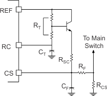
Slope compensation can be added in all current-mode control applications to cancel the peak-to-average current error. Slope compensation is necessary in applications with duty-cycles exceeding 50%, but also improves performance in those below 50%. Primary current is sensed using resistor RCS in series with the converter switch. The timing resistor can be broken up into two series resistors to bias up an NPN voltage-follower, as shown in Figure 32. This is required to provide ample compliance for slope compensation at the beginning of a switching cycle, especially with continuous-current converters. The voltage follower drives the slope compensating programming resistor (RSC) to provide a slope-compensating current into CF.
 Figure 32. Adding Slope Compensation