ZHCSKB9Q December 1999 – October 2019 UCC1895 , UCC2895 , UCC3895
PRODUCTION DATA.
- 1 特性
- 2 应用
- 3 说明
- 4 修订历史记录
- 5 Pin Configuration and Functions
- 6 Specifications
-
7 Detailed Description
- 7.1 Overview
- 7.2 Functional Block Diagrams
- 7.3
Feature Description
- 7.3.1 ADS (Adaptive Delay Set)
- 7.3.2 CS (Current Sense)
- 7.3.3 CT (Oscillator Timing Capacitor)
- 7.3.4 DELAB and DELCD (Delay Programming Between Complementary Outputs)
- 7.3.5 EAOUT, EAP, and EAN (Error Amplifier)
- 7.3.6 OUTA, OUTB, OUTC, and OUTD (Output MOSFET Drivers)
- 7.3.7 PGND (Power Ground)
- 7.3.8 RAMP (Inverting Input of the PWM Comparator)
- 7.3.9 REF (Voltage Reference)
- 7.3.10 RT (Oscillator Timing Resistor)
- 7.3.11 GND (Analog Ground)
- 7.3.12 SS/DISB (Soft Start/Disable)
- 7.3.13 SYNC (Oscillator Synchronization)
- 7.3.14 VDD (Chip Supply)
- 7.4 Device Functional Modes
- 7.5 Programming
-
8 Application and Implementation
- 8.1 Application Information
- 8.2
Typical Application
- 8.2.1 Design Requirements
- 8.2.2
Detailed Design Procedure
- 8.2.2.1 Power Loss Budget
- 8.2.2.2 Preliminary Transformer Calculations (T1)
- 8.2.2.3 QA, QB, QC, QD FET Selection
- 8.2.2.4 Selecting LS
- 8.2.2.5 Selecting Diodes DB and DC
- 8.2.2.6 Output Inductor Selection (LOUT)
- 8.2.2.7 Output Capacitance (COUT)
- 8.2.2.8 Select Rectifier Diodes
- 8.2.2.9 Input Capacitance (CIN)
- 8.2.2.10 Current Sense Network (CT, RCS, RR, DA)
- 8.2.3 Application Curves
- 9 Power Supply Recommendations
- 10Layout
- 11器件和文档支持
- 12机械、封装和可订购信息
封装选项
机械数据 (封装 | 引脚)
散热焊盘机械数据 (封装 | 引脚)
订购信息
8.2.2.2 Preliminary Transformer Calculations (T1)
Transformer turns ratio (a1):

The voltage drop across the RDS(on) of the primary side FETs is negligible. We assume a 0.5-V forward voltage drop in the output rectifiers.

Select transformer turns based on 70% duty cycle (DMAX) at minimum specified input voltage. This will give some room for dropout if a PFC front end is used.


Turns ratio rounded to the nearest whole turn.

Calculated typical duty cycle (DTYP) based on average input voltage.

Output inductor peak-to-peak ripple current is set to 20% of the output current.

Care must be taken in selecting the correct amount of magnetizing inductance (LMAG). The following equations calculate the minimum magnetizing inductance of the primary of the transformer (T1) to ensure the converter operates in current-mode control. As LMAG reduces, the increasing magnetizing current becomes an increasing proportion of the signal at the CS pin. If the magnetizing current increases enough it can swamp out the current sense signal across RCS and the converter will operate increasingly as if it were in voltage mode control rather than current mode.

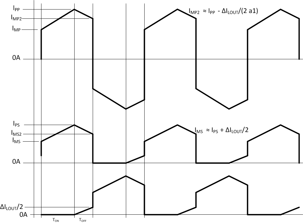
Figure 19 shows the transformer primary and secondary currents during normal operation.
 Figure 19. T1 Primary and Secondary Currents
 Calculate T1 secondary RMS current (ISRMS):


Secondary RMS current (ISRMS1) when energy is being delivered to the secondary: (OUTA = OUTD = HI or OUTB = OUTC = HI).

Secondary RMS current (ISRMS2) during freewheeling period: (OUTA = OUTC = HI or OUTB = OUTD = HI).

Secondary RMS current (ISRMS3) caused by the negative current in the opposing winding during freewheeling period, please refer to Figure 19.

Total secondary RMS current (ISRMS):

Calculate T1 Primary RMS Current (IPRMS):


T1 Primary RMS (IPRMS1) current when energy is being delivered to the secondary.

T1 Primary RMS (IPRMS2) current when the converter is free wheeling.

Total T1 primary RMS current (IPRMS):

We select a transformer with the following specifications:


Transformer Primary DC resistance:

Transformer Secondary DC resistance:

Estimated transformer core losses (PT1) are twice the copper loss.
NOTE
This is just an estimate and the total losses may vary based on magnetic design.

Calculate remaining power budget:
