ZHCSKB9Q December 1999 – October 2019 UCC1895 , UCC2895 , UCC3895
PRODUCTION DATA.
- 1 特性
- 2 应用
- 3 说明
- 4 修订历史记录
- 5 Pin Configuration and Functions
- 6 Specifications
-
7 Detailed Description
- 7.1 Overview
- 7.2 Functional Block Diagrams
- 7.3
Feature Description
- 7.3.1 ADS (Adaptive Delay Set)
- 7.3.2 CS (Current Sense)
- 7.3.3 CT (Oscillator Timing Capacitor)
- 7.3.4 DELAB and DELCD (Delay Programming Between Complementary Outputs)
- 7.3.5 EAOUT, EAP, and EAN (Error Amplifier)
- 7.3.6 OUTA, OUTB, OUTC, and OUTD (Output MOSFET Drivers)
- 7.3.7 PGND (Power Ground)
- 7.3.8 RAMP (Inverting Input of the PWM Comparator)
- 7.3.9 REF (Voltage Reference)
- 7.3.10 RT (Oscillator Timing Resistor)
- 7.3.11 GND (Analog Ground)
- 7.3.12 SS/DISB (Soft Start/Disable)
- 7.3.13 SYNC (Oscillator Synchronization)
- 7.3.14 VDD (Chip Supply)
- 7.4 Device Functional Modes
- 7.5 Programming
-
8 Application and Implementation
- 8.1 Application Information
- 8.2
Typical Application
- 8.2.1 Design Requirements
- 8.2.2
Detailed Design Procedure
- 8.2.2.1 Power Loss Budget
- 8.2.2.2 Preliminary Transformer Calculations (T1)
- 8.2.2.3 QA, QB, QC, QD FET Selection
- 8.2.2.4 Selecting LS
- 8.2.2.5 Selecting Diodes DB and DC
- 8.2.2.6 Output Inductor Selection (LOUT)
- 8.2.2.7 Output Capacitance (COUT)
- 8.2.2.8 Select Rectifier Diodes
- 8.2.2.9 Input Capacitance (CIN)
- 8.2.2.10 Current Sense Network (CT, RCS, RR, DA)
- 8.2.3 Application Curves
- 9 Power Supply Recommendations
- 10Layout
- 11器件和文档支持
- 12机械、封装和可订购信息
封装选项
机械数据 (封装 | 引脚)
散热焊盘机械数据 (封装 | 引脚)
订购信息
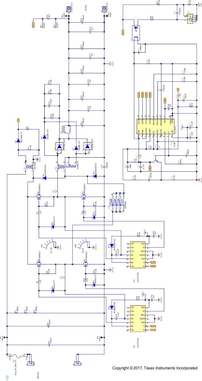
8.2.2.10.6 Setting the Slope Compensation
Slope compensation is necessary to stabilise a converter operating in peak current mode at duty cycles greater than 50%. The optimum slope compensation ramp should be half the inductor current ramp downslope during the off time. This slope is calculated as follows:

The magnetizing current of the power transformer provides part of the compensating ramp and is calculated as follows. The VIN x DTYP factor takes account of the fact that the slope of the magnetizing current is less at lower input voltages.

The added slope compensation ramp is then:

The resistor RSC sets the added slope compensation ramp, mSUM and is chosen as follows:

A small AC coupling capacitor is used in the emitter of Q1 to eliminate the need for offset biasing circuitry. CC = 1 nF.
The resistor REL is a DC load resistor for the emitter of Q1. It should have the same value as RSC.
A small capacitor at the RAMP pin input helps suppress high frequency noise, we set CRAMP = 56 pF. Transistor Q1 is a small signal NPN type.
In peak current mode control the RAMP pin receives the current sense signal, plus the slope compensation ramp, through the 510-Ω resistor RRCS. The 10-kΩ resistor RRB provides approximately 250-mV offset bias. The value of this resistor may be adjusted up or down to alter the point at which the internal no load comparator trips.
 Figure 24. Power Stage Schematic