SLUSDV5B October 2019 – April 2020 UCC5304
PRODUCTION DATA.
- 1 Features
- 2 Applications
- 3 Description
- 4 Revision History
- 5 Pin Configuration and Functions
-
6 Specifications
- 6.1 Absolute Maximum Ratings
- 6.2 ESD Ratings
- 6.3 Recommended Operating Conditions
- 6.4 Thermal Information
- 6.5 Power Ratings
- 6.6 Insulation Specifications
- 6.7 Safety-Related Certifications
- 6.8 Safety-Limiting Values
- 6.9 Electrical Characteristics
- 6.10 Switching Characteristics
- 6.11 Typical Characteristics
- 7 Parameter Measurement Information
- 8 Detailed Description
- 9 Application and Implementation
- 10Power Supply Recommendations
- 11Layout
- 12Mechanical, Packaging, and Orderable Information
8.3.1 VDD, VCCI, and Under Voltage Lock Out (UVLO)
The UCC5304 has an internal under voltage lock out (UVLO) protection feature on the supply circuit blocks between the VDD and VSS pins. When the VDD bias voltage is lower than VVDD_ON at device start-up or lower than VVDD_OFF after start-up, the VDD UVLO feature holds the effected output low, regardless of the status of the IN pin.
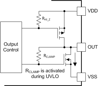
When the output stages of the driver are in an unbiased or UVLO condition, the driver outputs are held low by an active clamp circuit that limits the voltage rise on the driver outputs (Illustrated in Figure 20). In this condition, the upper PMOS is resistively held off by RHi-Z while the lower NMOS gate is tied to the driver output through RCLAMP. In this configuration, the output is effectively clamped to the threshold voltage of the lower NMOS device, typically around 1.5V, when no bias power is available.
 Figure 20. Simplified Representation of Active Pull Down Feature
 The VDD UVLO protection has a hysteresis feature (VVDD_HYS). This hysteresis prevents chatter when there is ground noise from the power supply. Also this allows the device to accept small drops in bias voltage, which is bound to happen when the device starts switching and operating current consumption increases suddenly.
The input side of the UCC5304 also has an internal under voltage lock out (UVLO) protection feature. The device isn't active unless the VCCI voltage exceeds VVCCI_ON on start up. The input signal will not be delivered when the VCCI suply is less than VVCCI_OFF. And, just like the UVLO for VDD, there is hystersis (VVCCI_HYS) to ensure stable operation.
Table 1. VCCI UVLO Feature Logic
| CONDITION | INPUT | OUTPUT |
| IN | OUT | |
| VCCI-GND < VVCCI_ON before device start up | H | L |
| VCCI-GND < VVCCI_ON before device start up | L | L |
| VCCI-GND < VVCCI_OFF after device start up | H | L |
| VCCI-GND < VVCCI_OFF after device start up | L | L |
Table 2. VDD UVLO Feature Logic
| CONDITION | INPUT | OUTPUT | |
| IN | OUT | ||
| VDD-VSS < VVDD_ON before device start up | H | L | |
| VDD-VSS < VVDD_ON before device start up | L | L | |
| VDD-VSS < VVDD_OFF after device start up | H | L | |
| VDD-VSS < VVDD_OFF after device start up | L | L | |