ZHCSMR1C october 2019 – september 2021 UCC5870-Q1
PRODUCTION DATA
- 1 特性
- 2 应用
- 3 说明
- 4 Revision History
- 5 Pin Configuration and Functions
- 6 Specifications
-
7 Detailed Description
- 7.1 Overview
- 7.2 Functional Block Diagram
- 7.3
Feature Description
- 7.3.1 Power Supplies
- 7.3.2 Driver Stage
- 7.3.3 Integrated ADC for Front-End Analog (FEA) Signal Processing
- 7.3.4 Fault and Warning Classification
- 7.3.5
Diagnostic Features
- 7.3.5.1 Undervoltage Lockout (UVLO) and Overvoltage Lockout (OVLO)
- 7.3.5.2 CLAMP, OUTH, and OUTL Clamping Circuits
- 7.3.5.3 Active Miller Clamp
- 7.3.5.4 DESAT based Short Circuit Protection (DESAT)
- 7.3.5.5 Shunt Resistor based Overcurrent Protection (OCP) and Short Circuit Protection (SCP)
- 7.3.5.6 Temperature Monitoring and Protection for the Power Transistors
- 7.3.5.7 Active High Voltage Clamping (VCECLP)
- 7.3.5.8 Two-Level Turn-Off
- 7.3.5.9 Soft Turn-Off (STO)
- 7.3.5.10 Thermal Shutdown (TSD) and Temperature Warning (TWN) of Driver IC
- 7.3.5.11 Active Short Circuit Support (ASC)
- 7.3.5.12 Shoot-Through Protection (STP)
- 7.3.5.13 Gate Voltage Monitoring and Status Feedback
- 7.3.5.14 VGTH Monitor
- 7.3.5.15 Cyclic Redundancy Check (CRC)
- 7.3.5.16 Configuration Data CRC
- 7.3.5.17 SPI Transfer Write/Read CRC
- 7.3.5.18 TRIM CRC Check
- 7.4 Device Functional Modes
- 7.5 Programming
- 7.6 Register Maps
- 8 Applications and Implementation
- 9 Power Supply Recommendations
- 10Layout
- 11Device and Documentation Support
- 12Mechanical, Packaging, and Orderable Information
7.3.5.1 Undervoltage Lockout (UVLO) and Overvoltage Lockout (OVLO)
UVLO functions are implemented for all three gate driver power supplies VCC1, VCC2, and VEE2. The VCC1 UVLO/OVLO ensures a valid supply is connected for the required logic interface. The UVLO/OVLO for VCC2 and VEE2 ensures valid supplies based on the type of transistor used. The UVLO function prevents overheating damage to the IGBTs/MOSFETs from being under-driven. The OVLO functions are implemented to prevent gate oxide degradation (shortened lifetime) of the IGBTs/MOSFETs from an over-voltage supply at turned on. The device powers up when a valid VCC1 supply (VIT+(UVLO1) < VVCC1 < VIT+(OVLO1)) and non-UV VCC2 supply (VVCC2 > VIT+(UVLO2)) are connected. The driver outputs are high impedance until the valid supplies are connected and the internal supplies are in regulation. While the driver output is high impedance, the output to the gate of the external power switch is held low with a passive and active pulldown circuit. See the Section 7.3.5.2 section for more details. Once valid supplies are connected and internal supplies are valid, the output state is determined by the Enable/Disable Driver command any fault conditions that exist. SPI communication is unavailable while VCC1 is lower than the UVLO1 threshold.
The OVLO and UVLO functions are enabled/disabled using the following bits: CFG1[UV1_DIS] for VCC1 UVLO, CFG1[OV1_DIS] for VCC1 OVLO, CFG4[UV2_DIS] for VCC2 UVLO,CFG4[OV2_DIS] for VCC2 OVLO, and CFG4[UVOV3_EN] for both the OVLO and UVLO for VEE2. The UVLO and OVLO thresholds for VCC1, VCC2 and VEE2 are programmable in order to customize the driver for different types of power transistors. Use the CFG1[UVLO1_LEVEL] and CFG1[OVLO1_LEVEL] (for VCC1), CFG7[UVLO2TH] and CFG7[OVLO2TH] (for VCC2), and CFG7[UVLO3TH] and CFG7[IOVLO3TH] (for VEE2) bits to set the desired threshold. See CFG1 and CFG7.
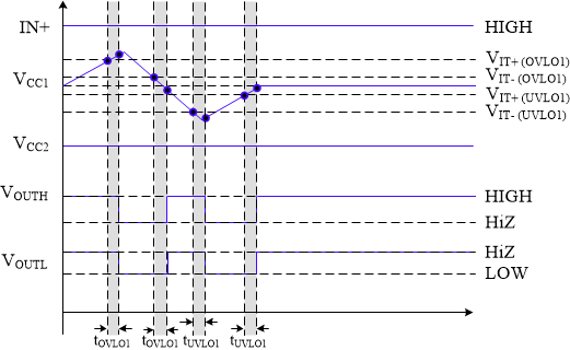
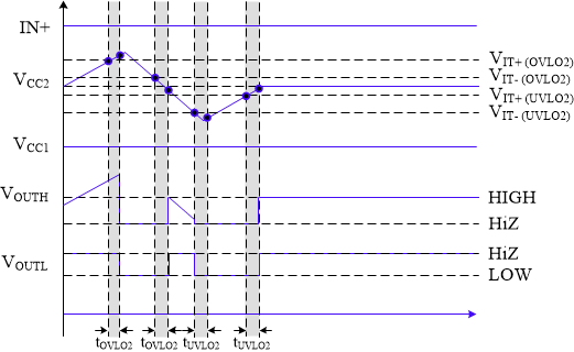
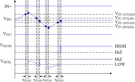
The fault status for the OVLO and UVLO function are located in STATUS2[UVLO1_FAULT] for VCC1 UVLO, STATUS2[OVLO1_FAULT] for VCC1 OVLO, STATUS3[UVLO2_FAULT] for VCC2 UVLO, STATUS3[OVLO2_FAULT] for VCC2 OVLO, STATUS3[UVLO3_FAULT] for VEE2 UVLO, and STATUS3[OVLO3_FAULT] for VEE2 OVLO. See STATUS2 and STATUS3 for additional details. The timing diagrams for the VCC1 and VCC2 UVLO and OVLO functions are shown in and Figure 7-10, respectively. The VEE2 timing diagram is shown in Figure 7-11.
 Figure 7-9 Illustration of UVLO and OVLO timing schemes of VCC1.
 Figure 7-10 Illustration of UVLO and OVLO timing schemes of VCC2
 Figure 7-11 Illustration of UVLO and OVLO timing schemes of VEE2