ZHCSMR1C october 2019 – september 2021 UCC5870-Q1
PRODUCTION DATA
- 1 特性
- 2 应用
- 3 说明
- 4 Revision History
- 5 Pin Configuration and Functions
- 6 Specifications
-
7 Detailed Description
- 7.1 Overview
- 7.2 Functional Block Diagram
- 7.3
Feature Description
- 7.3.1 Power Supplies
- 7.3.2 Driver Stage
- 7.3.3 Integrated ADC for Front-End Analog (FEA) Signal Processing
- 7.3.4 Fault and Warning Classification
- 7.3.5
Diagnostic Features
- 7.3.5.1 Undervoltage Lockout (UVLO) and Overvoltage Lockout (OVLO)
- 7.3.5.2 CLAMP, OUTH, and OUTL Clamping Circuits
- 7.3.5.3 Active Miller Clamp
- 7.3.5.4 DESAT based Short Circuit Protection (DESAT)
- 7.3.5.5 Shunt Resistor based Overcurrent Protection (OCP) and Short Circuit Protection (SCP)
- 7.3.5.6 Temperature Monitoring and Protection for the Power Transistors
- 7.3.5.7 Active High Voltage Clamping (VCECLP)
- 7.3.5.8 Two-Level Turn-Off
- 7.3.5.9 Soft Turn-Off (STO)
- 7.3.5.10 Thermal Shutdown (TSD) and Temperature Warning (TWN) of Driver IC
- 7.3.5.11 Active Short Circuit Support (ASC)
- 7.3.5.12 Shoot-Through Protection (STP)
- 7.3.5.13 Gate Voltage Monitoring and Status Feedback
- 7.3.5.14 VGTH Monitor
- 7.3.5.15 Cyclic Redundancy Check (CRC)
- 7.3.5.16 Configuration Data CRC
- 7.3.5.17 SPI Transfer Write/Read CRC
- 7.3.5.18 TRIM CRC Check
- 7.4 Device Functional Modes
- 7.5 Programming
- 7.6 Register Maps
- 8 Applications and Implementation
- 9 Power Supply Recommendations
- 10Layout
- 11Device and Documentation Support
- 12Mechanical, Packaging, and Orderable Information
7.3.5.13 Gate Voltage Monitoring and Status Feedback
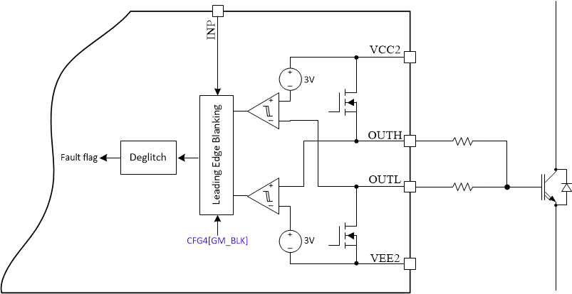
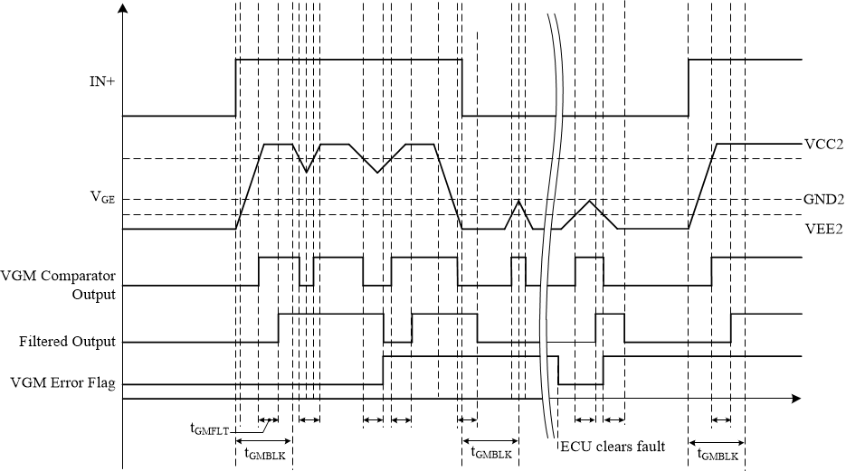
The integrity of the PWM channel is monitored end to end using two checks. The first check monitors the communication across the isolation channel. The received state on the secondary side is communicated back o the primary side to ensure the two match. If there is a mismatch between the IN+ state and the received IN+ state, the STATUS1[PWM_COMP_CHK_FAULT] bit (STATUS1) is set, if unmasked, nFLT1 pulls low, and the driver output is forced ot the state defined by CFG3[FS_STATE_PWM_CHK] (CFG3). The second check monitors the actual gate voltage of the power transistor to ensure the gate is in the correct state. The monitored gate voltage is first converted to logic state and indicated in the STATUS3[GM_STATE] bit (STATUS3). The converted gate voltage logic state is then compared with the input PWM (IN+) signal. The mismatch of the two signals causes a gate voltage monitor fault condition where the STATUS3[GM_FAULT] bit (STATUS3) is set, the driver output is forced to the state defined by CFG10[FS_STATE_GM] (CFG10), and, if unmasked, nFLT1 pulls low. Blanking time relative to the driver outputs is used to prevent false reporting of the gate voltage monitor error during driver transitions. During 2LTOFF transitions, the blanking time starts after the 2LTOFF plateau timer expires in order to prevent false GM faults during the transition. Alternatively, the GM fault may be disabled during STO and 2LTOFF using the CFG5[GM_STO2LTO_DIS] bit (CFG5). The blanking time is adjustable using the CFG4[GM_BLK] bits (CFG4). Additionally, the gate monitoring function may be disabled entirely using the CFG4[GM_EN] bit (CFG4). The implementation block diagram and timing schemes are presented in Figure 7-31 and Figure 7-32.
 Figure 7-31 Block diagram of implementation of
gate voltage monitor function.
 Figure 7-32 Timing scheme of implementation of
gate voltage monitor function.