ZHCSMR1C october 2019 – september 2021 UCC5870-Q1
PRODUCTION DATA
- 1 特性
- 2 应用
- 3 说明
- 4 Revision History
- 5 Pin Configuration and Functions
- 6 Specifications
-
7 Detailed Description
- 7.1 Overview
- 7.2 Functional Block Diagram
- 7.3
Feature Description
- 7.3.1 Power Supplies
- 7.3.2 Driver Stage
- 7.3.3 Integrated ADC for Front-End Analog (FEA) Signal Processing
- 7.3.4 Fault and Warning Classification
- 7.3.5
Diagnostic Features
- 7.3.5.1 Undervoltage Lockout (UVLO) and Overvoltage Lockout (OVLO)
- 7.3.5.2 CLAMP, OUTH, and OUTL Clamping Circuits
- 7.3.5.3 Active Miller Clamp
- 7.3.5.4 DESAT based Short Circuit Protection (DESAT)
- 7.3.5.5 Shunt Resistor based Overcurrent Protection (OCP) and Short Circuit Protection (SCP)
- 7.3.5.6 Temperature Monitoring and Protection for the Power Transistors
- 7.3.5.7 Active High Voltage Clamping (VCECLP)
- 7.3.5.8 Two-Level Turn-Off
- 7.3.5.9 Soft Turn-Off (STO)
- 7.3.5.10 Thermal Shutdown (TSD) and Temperature Warning (TWN) of Driver IC
- 7.3.5.11 Active Short Circuit Support (ASC)
- 7.3.5.12 Shoot-Through Protection (STP)
- 7.3.5.13 Gate Voltage Monitoring and Status Feedback
- 7.3.5.14 VGTH Monitor
- 7.3.5.15 Cyclic Redundancy Check (CRC)
- 7.3.5.16 Configuration Data CRC
- 7.3.5.17 SPI Transfer Write/Read CRC
- 7.3.5.18 TRIM CRC Check
- 7.4 Device Functional Modes
- 7.5 Programming
- 7.6 Register Maps
- 8 Applications and Implementation
- 9 Power Supply Recommendations
- 10Layout
- 11Device and Documentation Support
- 12Mechanical, Packaging, and Orderable Information
7.3.3 Integrated ADC for Front-End Analog (FEA) Signal Processing
A 10bit ADC is integrated to enable the user to digitally monitor up to 6 analog input voltages (AI*). Additionally, the junction temperature of the device is available as well as an input for measuring the VTH of the power FET. The ADC has a full scale voltage range of 0 to 3.6V, requiring 4V at VREF (either internal or external). The ADC conversions are aligned with the INP signal to ensure the least amount of noise coupling from the switching transients of the power transistors (TI proprietary). Once a conversion is complete, the conversion results are transferred to the primary side of the device with inter-die communication and the result is stored in the ADCDATA* registers. The last ADC result is always available in the register. Every ADC conversion is recorded with time stamp information for that conversion. The time stamp is the INP cycle where the measurement occurs. Once the ADC and the driver are enabled, the time stamp increments with every INP low to high edge. If a fault occurs, or the duty cycle is such that a transition is not seen on INP, the TIME_STAMP does not update.
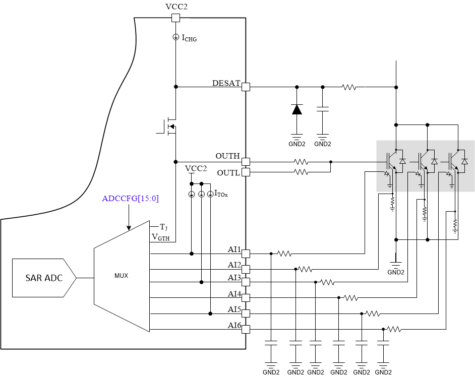
The AI* inputs are configurable by the user to enable/disable bias currents and comparator monitoring AI1, AI3, and AI5 are specially designed to monitor the temperature diode that is integrated into the power FET module, while A2, A4, and A6 are designed to measure the power FET current, typically from an integrated sense FET in the module. However, the inputs are not required to be used in these functions, and are configurable to measure any voltage up to 3.6V regardless of the source. The implementation of ADC sensing circuits is presented in Figure 7-3.
 Figure 7-3 Block diagram of implementation of ADC
processing for the case where three power transistors are connected in parallel.