ZHCS429J March   2012  – November 2021 UCD3138

PRODUCTION DATA  

  1. 特性
  2. 应用范围
  3. 说明
  4. 功能方框图
  5. Revision History
  6. Device Comparison Table
    1. 6.1 Product Family Comparison
    2. 6.2 Product Selection Matrix
  7. Pin Configuration and Functions
    1. 7.1 UCD3138RGC 64 QFN Pin Attributes
    2. 7.2 UCD3138RHA, UCD3138RMH and UCD3138RJA Pin Attributes
  8. Specifications
    1. 8.1 Absolute Maximum Ratings
    2. 8.2 ESD Ratings
    3. 8.3 Recommended Operating Conditions
    4. 8.4 Thermal Information
    5. 8.5 Electrical Characteristics
    6. 8.6 Timing and Switching Characteristics
    7. 8.7 Power Supply Sequencing
    8. 8.8 Peripherals
      1. 8.8.1 Digital Power Peripherals (DPPs)
        1. 8.8.1.1 Front End
        2. 8.8.1.2 DPWM Module
        3. 8.8.1.3 DPWM Events
        4. 8.8.1.4 High Resolution DPWM
        5. 8.8.1.5 Oversampling
        6. 8.8.1.6 DPWM Interrupt Generation
        7. 8.8.1.7 DPWM Interrupt Scaling/Range
    9. 8.9 Typical Temperature Characteristics
  9. Detailed Description
    1. 9.1 Overview
    2. 9.2 ARM Processor
    3. 9.3 Memory
      1. 9.3.1 CPU Memory Map and Interrupts
      2. 9.3.2 Boot ROM
      3. 9.3.3 Customer Boot Program
      4. 9.3.4 Flash Management
    4. 9.4 System Module
      1. 9.4.1 Address Decoder (DEC)
      2. 9.4.2 Memory Management Controller (MMC)
      3. 9.4.3 System Management (SYS)
      4. 9.4.4 Central Interrupt Module (CIM)
    5. 9.5 Feature Description
      1. 9.5.1  Sync FET Ramp and IDE Calculation
      2. 9.5.2  Automatic Mode Switching
        1. 9.5.2.1 Phase Shifted Full Bridge Example
        2. 9.5.2.2 LLC Example
        3. 9.5.2.3 Mechanism for Automatic Mode Switching
      3. 9.5.3  DPWMC, Edge Generation, IntraMux
      4. 9.5.4  Filter
        1. 9.5.4.1 Loop Multiplexer
        2. 9.5.4.2 Fault Multiplexer
      5. 9.5.5  Communication Ports
        1. 9.5.5.1 SCI (UART) Serial Communication Interface
        2. 9.5.5.2 PMBUS
        3. 9.5.5.3 General Purpose ADC12
        4. 9.5.5.4 Timers
          1. 9.5.5.4.1 24-bit PWM Timer
          2. 9.5.5.4.2 16-Bit PWM Timers
          3. 9.5.5.4.3 Watchdog Timer
      6. 9.5.6  Miscellaneous Analog
      7. 9.5.7  Package ID Information
      8. 9.5.8  Brownout
      9. 9.5.9  Global I/O
      10. 9.5.10 Temperature Sensor Control
      11. 9.5.11 I/O Mux Control
      12. 9.5.12 Current Sharing Control
      13. 9.5.13 Temperature Reference
    6. 9.6 Device Functional Modes
      1. 9.6.1 Normal Mode
      2. 9.6.2 Phase Shifting
      3. 9.6.3 DPWM Multiple Output Mode
      4. 9.6.4 DPWM Resonant Mode
      5. 9.6.5 Triangular Mode
      6. 9.6.6 Leading Edge Mode
  10. 10Application and Implementation
    1. 10.1 Application Information
    2. 10.2 Typical Application
      1. 10.2.1 Design Requirements
      2. 10.2.2 Detailed Design Procedure
        1. 10.2.2.1 PCMC (Peak Current Mode Control) PSFB (Phase Shifted Full Bridge) Hardware Configuration Overview
        2. 10.2.2.2 DPWM Initialization for PSFB
        3. 10.2.2.3 DPWM Synchronization
        4. 10.2.2.4 Fixed Signals to Bridge
        5. 10.2.2.5 Dynamic Signals to Bridge
        6. 10.2.2.6 System Initialization for PCM
          1. 10.2.2.6.1 Use of Front Ends and Filters in PSFB
          2. 10.2.2.6.2 Peak Current Detection
          3. 10.2.2.6.3 Peak Current Mode (PCM)
      3. 10.2.3 Application Curves
  11. 11Power Supply Recommendations
    1. 11.1 Introduction To Power Supply and Layout Recommendations
    2. 11.2 3.3-V Supply Pins
    3. 11.3 Recommendation for V33 Ramp up Slew Rate for UCD3138 and UCD3138064
    4. 11.4 Recommendation for RC Time Constant of RESET Pin for UCD3138 and UCD3138064
  12. 12Layout
    1. 12.1 Layout Guidelines
      1. 12.1.1 EMI and EMC Mitigation Guidelines
      2. 12.1.2 BP18 Pin
      3. 12.1.3 Additional Bias Guidelines
      4. 12.1.4 UCD3138 Pin Connection Recommendation
        1. 12.1.4.1 Current Amplifier With EADC Connection
        2. 12.1.4.2 DPWM Synchronization
        3. 12.1.4.3 GPIOS
        4. 12.1.4.4 DPWM PINS
        5. 12.1.4.5 EAP and EAN Pins
        6. 12.1.4.6 ADC Pins
      5. 12.1.5 UART Communication Port
      6. 12.1.6 Special Considerations
    2. 12.2 Layout Example
      1. 12.2.1 UCD3138 and UCD3138064 40 Pin
      2. 12.2.2 UCD3138 and UCD3138064 64 Pin
  13. 13Device and Documentation Support
    1. 13.1 Device Support
      1. 13.1.1 Code Composer Studio
      2. 13.1.2 Tools and Documentation
    2. 13.2 Documentation Support
      1. 13.2.1 References
    3. 13.3 接收文档更新通知
    4. 13.4 支持资源
    5. 13.5 Trademarks
    6. 13.6 Electrostatic Discharge Caution
    7. 13.7 术语表
  14. 14Mechanical Packaging and Orderable Information
    1. 14.1 Packaging Information

封装选项

机械数据 (封装 | 引脚)
散热焊盘机械数据 (封装 | 引脚)
订购信息

Current Sharing Control

UCD3138 provides three separate modes of current sharing operation.

  • Analog bus current sharing
  • PWM bus current sharing
  • Master/Slave current sharing
  • AD02 has a special ESD protection mechanism that prevents the pin from pulling down the current-share bus if power is missing from the UCD3138

The simplified current sharing circuitry is shown in the drawing below:
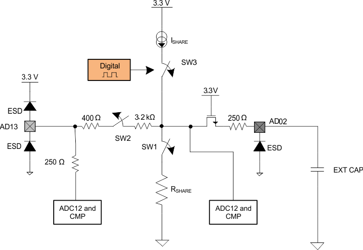
GUID-0086E1F7-6A68-43EB-AB10-1C35D46D0316-low.gifFigure 9-16 Simplified Current Sharing Circuitry
CURRENT SHARING MODEFOR TEST ONLY,
ALWAYS KEEP 00
CS_MODEEN_SW1EN_SW2DPWM
Off or Slave Mode (3-state)0000 (default)000
PWM Bus000110ACTIVE
Off or Slave Mode (3-state)0010000
Analog Bus or Master0011010

The period and the duty of 8-bit PWM current source and the state of the SW1 and SW2 switches can be controlled through the current sharing control register (CSCTRL).