ZHCSAY5D
march 2013 – april 2021
UCD3138064
PRODUCTION DATA
1
特性
2
应用
3
说明
4
Functional Block Diagram
5
Revision History
6
Device Options
6.1
Device Comparison Table
6.2
Product Selection Matrix
7
Pin Configuration and Functions
7.1
Pin Diagrams
7.2
Pin Functions
8
Specifications
8.1
Absolute Maximum Ratings #GUID-DB56AA00-A5E9-4426-9853-ACC9CCD10656/SLUSB727999
8.2
Handling Ratings
8.3
Recommended Operating Conditions
8.4
Thermal Information
8.5
Electrical Characteristics
8.6
Timing Characteristics
8.7
PMBus/SMBus/I2C Timing
8.8
Power On Reset (POR) / Brown Out Reset (BOR)
8.9
Typical Clock Gating Power Savings
8.10
Typical Characteristics
9
Detailed Description
9.1
Overview
9.1.1
ARM Processor
9.1.2
Memory
9.2
Functional Block Diagram
9.3
Feature Description
9.3.1
System Module
9.3.1.1
Address Decoder (DEC)
9.3.1.2
Memory Management Controller (MMC)
9.3.1.3
System Management (SYS)
9.3.1.4
Central Interrupt Module (CIM)
9.3.2
Peripherals
9.3.2.1
Digital Power Peripherals
9.3.2.1.1
Front End
9.3.2.1.2
DPWM Module
9.3.2.1.3
DPWM Events
9.3.2.1.4
High Resolution DPWM
9.3.2.1.5
Over Sampling
9.3.2.1.6
DPWM Interrupt Generation
9.3.2.1.7
DPWM Interrupt Scaling/Range
9.3.3
Automatic Mode Switching
9.3.3.1
Phase Shifted Full Bridge Example
9.3.3.2
LLC Example
9.3.3.3
Mechanism For Automatic Mode Switching
9.3.4
DPWMC, Edge Generation, Intramux
9.3.5
Filter
9.3.5.1
Loop Multiplexer
9.3.5.2
Fault Multiplexer
9.3.6
Communication Ports
9.3.6.1
SCI (UART) Serial Communication Interface
9.3.6.2
PMBUS/I2C
9.3.6.3
SPI
9.3.7
Real Time Clock
9.3.8
Timers
9.3.8.1
24-Bit Timer
9.3.8.2
16-Bit PWM Timers
9.3.8.3
Watchdog Timer
9.3.9
General Purpose ADC12
9.3.10
Miscellaneous Analog
9.3.11
Brownout
9.3.12
Global I/O
9.3.13
Temperature Sensor Control
9.3.14
I/O Mux Control
9.3.15
Current Sharing Control
9.3.16
Temperature Reference
9.4
Device Functional Modes
9.4.1
DPWM Modes Of Operation
9.4.1.1
Normal Mode
9.4.1.2
Phase Shifting
9.4.1.3
DPWM Multiple Output Mode
9.4.1.4
DPWM Resonant Mode
9.4.2
Triangular Mode
9.4.3
Leading Edge Mode
9.5
Memory
9.5.1
Register Maps
9.5.1.1
CPU Memory Map and Interrupts
9.5.1.1.1
Memory Map (After Reset Operation)
9.5.1.1.2
Memory Map (Normal Operation)
9.5.1.1.3
Memory Map (System and Peripherals Blocks)
9.5.1.2
Boot ROM
9.5.1.3
Customer Boot Program
9.5.1.4
Flash Management
9.5.1.5
Synchronous Rectifier MOSFET Ramp and IDE Calculation
10
Applications and Implementation
10.1
Application Information
10.2
Typical Application
10.2.1
Design Requirements
10.2.2
Detailed Design Procedure
10.2.2.1
PCMC (Peak Current Mode Control) PSFB (Phase Shifted Full Bridge) Hardware Configuration Overview
10.2.2.2
DPWM Initialization for PSFB
10.2.2.2.1
DPWM Synchronization
10.2.2.3
Fixed Signals to Bridge
10.2.2.4
Dynamic Signals to Bridge
10.2.2.5
System Initialization for PCM
10.2.2.5.1
Use of Front Ends and Filters in PSFB
10.2.2.5.2
Peak Current Detection
10.2.2.5.3
Peak Current Mode (PCM)
10.2.3
Application Curves
11
Power Supply Recommendations
11.1
Introduction To Power Supply and Layout Recommendations
11.2
3.3-V Supply Pins
11.3
Recommendation for V33 Ramp up Slew Rate for UCD3138 and UCD3138064
11.4
Recommendation for RC Time Constant of RESET Pin for UCD3138 and UCD3138064
12
Layout
12.1
Layout Guidelines
12.1.1
EMI and EMC Mitigation Guidelines
12.1.2
BP18 Pin
12.1.3
Additional Bias Guidelines
UCD3138 Pin Connection Recommendation
12.1.4.1
Current Amplifier With EADC Connection
12.1.4.2
DPWM Synchronization
12.1.4.3
External Clock
12.1.4.4
GPIOS
12.1.4.5
DPWM PINS
12.1.4.6
EAP and EAN Pins
12.1.4.7
ADC Pins
12.1.4.7.1
RESET Pin
12.1.4
UART Communication Port
Special Considerations
12.2
Layout Example
12.2.1
UCD3138 and UCD3138064 40 Pin
12.2.2
UCD3138 and UCD3138064 64 Pin
13
Device and Documentation Support
13.1
Device Support
13.2
Documentation Support
13.2.1
Related Documentation
13.3
Trademarks
13.4
静电放电警告
13.5
术语表
14
Mechanical, Packaging, and Orderable Information
封装选项
机械数据 (封装 | 引脚)
RJA|40
MPQF467A
RMH|40
MPQF388A
RGC|64
MPQF125F
散热焊盘机械数据 (封装 | 引脚)
RJA|40
QFND826
RGC|64
QFND102O
订购信息
zhcsay5d_oa
zhcsay5d_pm
4
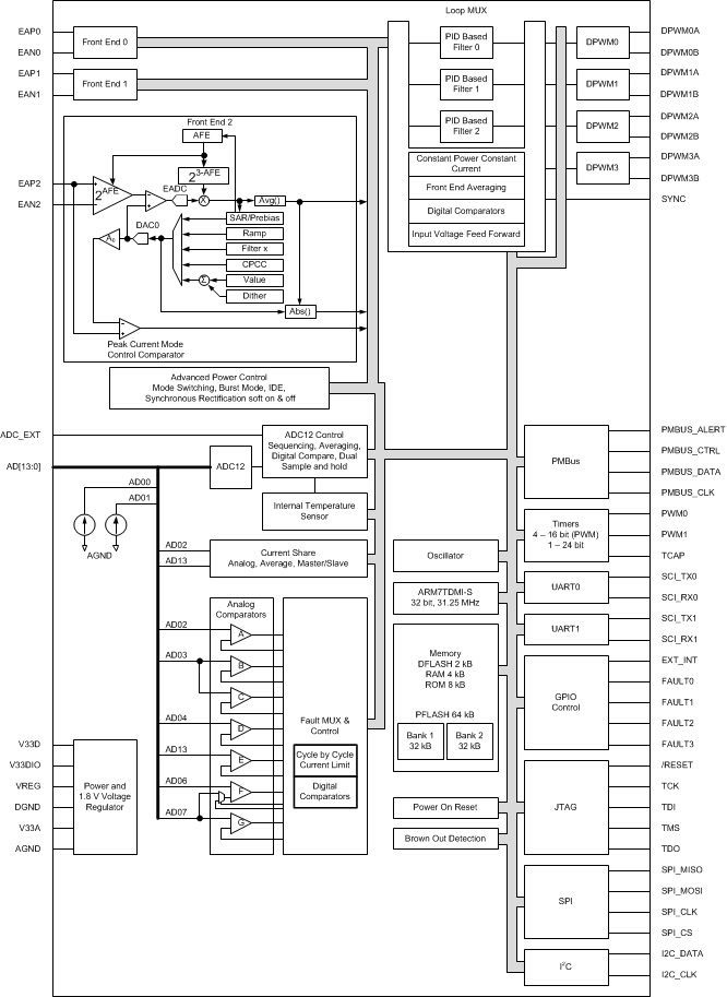
Functional Block Diagram
千亿体育app官网登录(中国)官方网站IOS/安卓通用版/手机APP
|
米乐app下载官网(中国)|ios|Android/通用版APP最新版
|
米乐|米乐·M6(中国大陆)官方网站
|
千亿体育登陆地址
|
华体会体育(中国)HTH·官方网站
|
千赢qy国际_全站最新版千赢qy国际V6.2.14安卓/IOS下载
|
18新利网v1.2.5|中国官方网站
|
bob电竞真人(中国官网)安卓/ios苹果/电脑版【1.97.95版下载】
|
千亿体育app官方下载(中国)官方网站IOS/安卓/手机APP下载安装
|