ZHCSAY5D march 2013 – april 2021 UCD3138064
PRODUCTION DATA
- 1 特性
- 2 应用
- 3 说明
- 4 Functional Block Diagram
- 5 Revision History
- 6 Device Options
- 7 Pin Configuration and Functions
-
8 Specifications
- 8.1 Absolute Maximum Ratings #GUID-DB56AA00-A5E9-4426-9853-ACC9CCD10656/SLUSB727999
- 8.2 Handling Ratings
- 8.3 Recommended Operating Conditions
- 8.4 Thermal Information
- 8.5 Electrical Characteristics
- 8.6 Timing Characteristics
- 8.7 PMBus/SMBus/I2C Timing
- 8.8 Power On Reset (POR) / Brown Out Reset (BOR)
- 8.9 Typical Clock Gating Power Savings
- 8.10 Typical Characteristics
-
9 Detailed Description
- 9.1 Overview
- 9.2 Functional Block Diagram
- 9.3
Feature Description
- 9.3.1 System Module
- 9.3.2 Peripherals
- 9.3.3 Automatic Mode Switching
- 9.3.4 DPWMC, Edge Generation, Intramux
- 9.3.5 Filter
- 9.3.6 Communication Ports
- 9.3.7 Real Time Clock
- 9.3.8 Timers
- 9.3.9 General Purpose ADC12
- 9.3.10 Miscellaneous Analog
- 9.3.11 Brownout
- 9.3.12 Global I/O
- 9.3.13 Temperature Sensor Control
- 9.3.14 I/O Mux Control
- 9.3.15 Current Sharing Control
- 9.3.16 Temperature Reference
- 9.4 Device Functional Modes
- 9.5 Memory
-
10Applications and
Implementation
- 10.1 Application Information
- 10.2
Typical Application
- 10.2.1 Design Requirements
- 10.2.2 Detailed Design Procedure
- 10.2.3 Application Curves
- 11Power Supply Recommendations
- 12Layout
- 13Device and Documentation Support
- 14Mechanical, Packaging, and Orderable Information
封装选项
机械数据 (封装 | 引脚)
散热焊盘机械数据 (封装 | 引脚)
订购信息
9.3.4 DPWMC, Edge Generation, Intramux
The UCD3138x has hardware for generating complex waveforms beyond the simple DPWMA and DPWMB waveforms already discussed – DPWMC, the Edge Generation Module, and the IntraMux.
DPWMC is a signal inside the DPWM logic. It goes high at the Blanking A begin time, and low at the Blanking A end time.
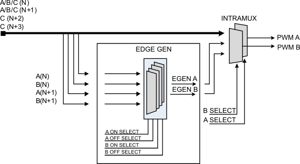
The Edge Gen module takes DPWMA and DPWMB from its own DPWM module, and the next one, and uses them to generate edges for two outputs. For DPWM3, the DPWM0 is considered to be the next DPWM. Each edge (rising and falling for DPWMA and DPWMB) has 8 options which can cause it.
The options are:
0 = DPWM(n) A Rising edge
1 = DPWM(n) A Falling edge
2 = DPWM(n) B Rising edge
3 = DPWM(n) B Falling edge
4 = DPWM(n+1) A Rising edge
5 = DPWM(n+1) A Falling edge
6 = DPWM(n+1) B Rising edge
7 = DPWM(n+1) B Falling edge
Where “n" is the numerical index of the DPWM module of interest. For example n=1 refers to DPWM1.
The Edge Gen is controlled by the DPWMEDGEGEN register. It also has an enable/disable bit.
The IntraMux is controlled by the Auto Config registers. Intra Mux is short for intra multiplexer. The IntraMux takes signals from multiple DPWMs and from the Edge Gen and combines them logically to generate DPWMA and DPWMB signals This is useful for topologies like phase-shifted full bridge, especially when they are controlled with automatic mode switching. Of course, it can all be disabled, and DPWMA and DPWMB will be driven as described in the sections above. If the Intra Mux is enabled, high resolution must be disabled, and DPWM edge resolution goes down to 4 ns.
Here is a drawing of the Edge Gen/Intra Mux:
 Figure 9-9 Edge Generation / IntraMux
Here is a list of the IntraMux modes for DPWMA:
0 = DPWMA(n) pass through (default)
1 = Edge-gen output, DPWMA(n)
2 = DPWNC(n)
3 = DPWMB(n) (Crossover)
4 = DPWMA(n+1)
5 = DPWMB(n+1)
6 = DPWMC(n+1)
7 = DPWMC(n+2)
8 = DPWMC(n+3)
0 = DPWMB(n) pass through (default)
1 = Edge-gen output, DPWMB(n)
2 = DPWNC(n)
3 = DPWMA(n) (Crossover)
4 = DPWMA(n+1)
5 = DPWMB(n+1)
6 = DPWMC(n+1)
7 = DPWMC(n+2)
8 = DPWMC(n+3)
The DPWM number wraps around just like the Edge Gen unit. For DPWM3 the following definitions apply:
| DPWM(n) | DPWM3 |
| DPWM(n+1) | DPWM0 |
| DPWM(n+2) | DPWM1 |
| DPWM(n+3) | DPWM2 |