ZHCSAY5D march   2013  – april 2021 UCD3138064

PRODUCTION DATA  

  1. 特性
  2. 应用
  3. 说明
  4. Functional Block Diagram
  5. Revision History
  6. Device Options
    1. 6.1 Device Comparison Table
    2. 6.2 Product Selection Matrix
  7. Pin Configuration and Functions
    1. 7.1 Pin Diagrams
    2. 7.2 Pin Functions
  8. Specifications
    1. 8.1  Absolute Maximum Ratings #GUID-DB56AA00-A5E9-4426-9853-ACC9CCD10656/SLUSB727999
    2. 8.2  Handling Ratings
    3. 8.3  Recommended Operating Conditions
    4. 8.4  Thermal Information
    5. 8.5  Electrical Characteristics
    6. 8.6  Timing Characteristics
    7. 8.7  PMBus/SMBus/I2C Timing
    8. 8.8  Power On Reset (POR) / Brown Out Reset (BOR)
    9. 8.9  Typical Clock Gating Power Savings
    10. 8.10 Typical Characteristics
  9. Detailed Description
    1. 9.1 Overview
      1. 9.1.1 ARM Processor
      2. 9.1.2 Memory
    2. 9.2 Functional Block Diagram
    3. 9.3 Feature Description
      1. 9.3.1  System Module
        1. 9.3.1.1 Address Decoder (DEC)
        2. 9.3.1.2 Memory Management Controller (MMC)
        3. 9.3.1.3 System Management (SYS)
        4. 9.3.1.4 Central Interrupt Module (CIM)
      2. 9.3.2  Peripherals
        1. 9.3.2.1 Digital Power Peripherals
          1. 9.3.2.1.1 Front End
          2. 9.3.2.1.2 DPWM Module
          3. 9.3.2.1.3 DPWM Events
          4. 9.3.2.1.4 High Resolution DPWM
          5. 9.3.2.1.5 Over Sampling
          6. 9.3.2.1.6 DPWM Interrupt Generation
          7. 9.3.2.1.7 DPWM Interrupt Scaling/Range
      3. 9.3.3  Automatic Mode Switching
        1. 9.3.3.1 Phase Shifted Full Bridge Example
        2. 9.3.3.2 LLC Example
        3. 9.3.3.3 Mechanism For Automatic Mode Switching
      4. 9.3.4  DPWMC, Edge Generation, Intramux
      5. 9.3.5  Filter
        1. 9.3.5.1 Loop Multiplexer
        2. 9.3.5.2 Fault Multiplexer
      6. 9.3.6  Communication Ports
        1. 9.3.6.1 SCI (UART) Serial Communication Interface
        2. 9.3.6.2 PMBUS/I2C
        3. 9.3.6.3 SPI
      7. 9.3.7  Real Time Clock
      8. 9.3.8  Timers
        1. 9.3.8.1 24-Bit Timer
        2. 9.3.8.2 16-Bit PWM Timers
        3. 9.3.8.3 Watchdog Timer
      9. 9.3.9  General Purpose ADC12
      10. 9.3.10 Miscellaneous Analog
      11. 9.3.11 Brownout
      12. 9.3.12 Global I/O
      13. 9.3.13 Temperature Sensor Control
      14. 9.3.14 I/O Mux Control
      15. 9.3.15 Current Sharing Control
      16. 9.3.16 Temperature Reference
    4. 9.4 Device Functional Modes
      1. 9.4.1 DPWM Modes Of Operation
        1. 9.4.1.1 Normal Mode
        2. 9.4.1.2 Phase Shifting
        3. 9.4.1.3 DPWM Multiple Output Mode
        4. 9.4.1.4 DPWM Resonant Mode
      2. 9.4.2 Triangular Mode
      3. 9.4.3 Leading Edge Mode
    5. 9.5 Memory
      1. 9.5.1 Register Maps
        1. 9.5.1.1 CPU Memory Map and Interrupts
          1. 9.5.1.1.1 Memory Map (After Reset Operation)
          2. 9.5.1.1.2 Memory Map (Normal Operation)
          3. 9.5.1.1.3 Memory Map (System and Peripherals Blocks)
        2. 9.5.1.2 Boot ROM
        3. 9.5.1.3 Customer Boot Program
        4. 9.5.1.4 Flash Management
        5. 9.5.1.5 Synchronous Rectifier MOSFET Ramp and IDE Calculation
  10. 10Applications and Implementation
    1. 10.1 Application Information
    2. 10.2 Typical Application
      1. 10.2.1 Design Requirements
      2. 10.2.2 Detailed Design Procedure
        1. 10.2.2.1 PCMC (Peak Current Mode Control) PSFB (Phase Shifted Full Bridge) Hardware Configuration Overview
        2. 10.2.2.2 DPWM Initialization for PSFB
          1. 10.2.2.2.1 DPWM Synchronization
        3. 10.2.2.3 Fixed Signals to Bridge
        4. 10.2.2.4 Dynamic Signals to Bridge
        5. 10.2.2.5 System Initialization for PCM
          1. 10.2.2.5.1 Use of Front Ends and Filters in PSFB
          2. 10.2.2.5.2 Peak Current Detection
          3. 10.2.2.5.3 Peak Current Mode (PCM)
      3. 10.2.3 Application Curves
  11. 11Power Supply Recommendations
    1. 11.1 Introduction To Power Supply and Layout Recommendations
    2. 11.2 3.3-V Supply Pins
    3. 11.3 Recommendation for V33 Ramp up Slew Rate for UCD3138 and UCD3138064
    4. 11.4 Recommendation for RC Time Constant of RESET Pin for UCD3138 and UCD3138064
  12. 12Layout
    1. 12.1 Layout Guidelines
      1. 12.1.1 EMI and EMC Mitigation Guidelines
      2. 12.1.2 BP18 Pin
      3. 12.1.3 Additional Bias Guidelines
      4.      UCD3138 Pin Connection Recommendation
        1. 12.1.4.1 Current Amplifier With EADC Connection
        2. 12.1.4.2 DPWM Synchronization
        3. 12.1.4.3 External Clock
        4. 12.1.4.4 GPIOS
        5. 12.1.4.5 DPWM PINS
        6. 12.1.4.6 EAP and EAN Pins
        7. 12.1.4.7 ADC Pins
          1. 12.1.4.7.1 RESET Pin
      5. 12.1.4 UART Communication Port
      6.      Special Considerations
    2. 12.2 Layout Example
      1. 12.2.1 UCD3138 and UCD3138064 40 Pin
      2. 12.2.2 UCD3138 and UCD3138064 64 Pin
  13. 13Device and Documentation Support
    1. 13.1 Device Support
    2. 13.2 Documentation Support
      1. 13.2.1 Related Documentation
    3. 13.3 Trademarks
    4. 13.4 静电放电警告
    5. 13.5 术语表
  14. 14Mechanical, Packaging, and Orderable Information

封装选项

机械数据 (封装 | 引脚)
散热焊盘机械数据 (封装 | 引脚)
订购信息
DPWM Events

Each DPWM can control the following timing events:

  1. Sample Trigger Count–This register defines where the error voltage is sampled by the EADC in relationship to the DPWM period. The programmed value set in the register should be one fourth of the value calculated based on the DPWM clock. As the DCLK (DCLK = 62.5 MHz max) controlling the circuitry runs at one fourth of the DPWM clock (PCLK = 250MHz max). When this sample trigger count is equal to the DPWM Counter, it initiates a front end calculation by triggering the EADC, resulting in a CLA calculation, and a DPWM update. Over-sampling can be set for 2, 4 or 8 times the sampling rate.
  2. Phase Trigger Count–count offset for slaving another DPWM (Multi-Phase/Interleaved operation).
  3. Period–low resolution switching period count. (count of PCLK cycles)
  4. Event 1–count offset for rising DPWM A event. (PCLK cycles)
  5. Event 2–DPWM count for falling DPWM A event that sets the duty ratio. Last 4 bits of the register are for high resolution control. Upper 14 bits are the number of PCLK cycle counts.
  6. Event 3–DPWM count for rising DPWM B event. Last 4 bits of the register are for high resolution control. Upper 14 bits are the number of PCLK cycle counts.
  7. Event 4–DPWM count for falling DPWM B event. Last 4 bits of the register are for high resolution control. Upper 14 bits are the number of PCLK cycle counts.
  8. Cycle Adjust–Constant offset for Event 2 and Event 4 adjustments.

Basic comparisons between the programmed registers and the DPWM counter can create the desired edge placements in the DPWM. High resolution edge capability is available on Events 2, 3 and 4.
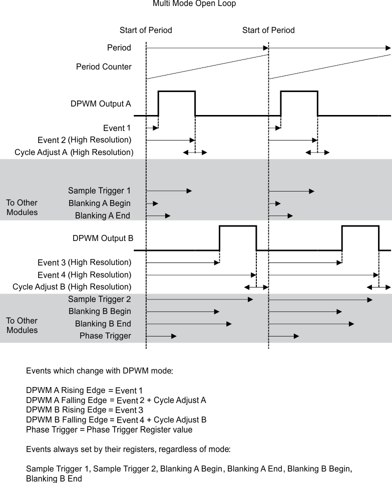
GUID-DA3EEC72-964A-4D11-BEE3-E1AA0200DE2C-low.gifFigure 9-3 Multi Mode Open Loop

Figure 9-3 is for multi-mode, open loop. Open loop means that the DPWM is controlled entirely by its own registers, not by the filter output. In other words, the power supply control loop is not closed.

The Sample Trigger signals are used to trigger the Front End to sample input signals. The Blanking signals are used to blank fault measurements during noisy events, such as FET turn on and turn off. Additional DPWM modes are described below.