ZHCSDJ8A March 2015 – April 2015 UCD3138A
PRODUCTION DATA.
- 1器件概述
- 2修订历史记录
- 3Device Comparison
- 4Terminal Configuration and Functions
- 5Specifications
-
6Detailed Description
- 6.1 Overview
- 6.2 ARM Processor
- 6.3 Memory
- 6.4 System Module
- 6.5 DPWM Modes of Operation
- 6.6 Sync FET Ramp and IDE Calculation
- 6.7 Automatic Mode Switching
- 6.8 DPWMC, Edge Generation, IntraMux
- 6.9 Filter
- 6.10 Communication Ports
- 6.11 Miscellaneous Analog
- 6.12 Package ID Information
- 6.13 Brownout
- 6.14 Global I/O
- 6.15 Temperature Sensor Control
- 6.16 I/O Mux Control
- 6.17 Current Sharing Control
- 6.18 Temperature Reference
-
7Application, Implementation, and Layout
- 7.1 Application Information
- 7.2 Typical Application
- 7.3 Layout
- 7.4 Power Supply Decoupling and Bulk Capacitors
- 8器件和文档支持
- 9机械封装和可订购信息
封装选项
机械数据 (封装 | 引脚)
散热焊盘机械数据 (封装 | 引脚)
订购信息
5 Specifications
5.1 Absolute Maximum Ratings(1)
over operating free-air temperature range (unless otherwise noted)| MIN | MAX | UNIT | ||
|---|---|---|---|---|
| Voltage | V33D to DGND | –0.3 | 3.8 | V |
| V33DIO to DGND | –0.3 | 3.8 | V | |
| V33A to AGND | –0.3 | 3.8 | V | |
| BP18 to DGND | –0.3 | 2.5 | V | |
| Ground difference, |DGND – AGND| | 0.3 | V | ||
| Applied to all pins, excluding AGND (2) | –0.3 | 3.8 | V | |
| Junction temperature, TJ | –40 | 150 | °C | |
| Storage temperature, Tstg | –55 | 150 | °C | |
5.2 ESD Ratings
| VALUE | UNIT | |||
|---|---|---|---|---|
| V(ESD) | Electrostatic discharge | Human-body model (HBM), per ANSI/ESDA/JEDEC JS-001(1) | ±2000 | V |
| Charged-device model (CDM), per JEDEC specification JESD22-C101(2) | ±500 | |||
5.3 Recommended Operating Conditions
over operating free-air temperature range (unless otherwise noted)| MIN | NOM | MAX | UNIT | ||
|---|---|---|---|---|---|
| Digital power, V33D | 3 | 3.3 | 3.6 | V | |
| Digital I/O power, V33DIO | 3 | 3.3 | 3.6 | ||
| Analog power, V33A | 3 | 3.3 | 3.6 | V | |
| Junction temperature, TJ | –40 | 125 | °C | ||
| 1.8-V digital power, BP18 | 1.6 | 1.8 | 2 | V |
5.4 Electrical Characteristics
V33A = V33D = V33DIO = 3 V to 3.6 V; 1 μF from BP18 to DGND, TJ = –40°C to 125°C (unless otherwise noted)| PARAMETER | TEST CONDITION | MIN | TYP | MAX | UNIT | |
|---|---|---|---|---|---|---|
| SUPPLY CURRENT | ||||||
| I33A | Measured on V33A. The device is powered up but all ADC12 and EADC sampling is disabled | 6.3 | mA | |||
| I33DIO | All GPIO and communication pins are open | 0.35 | mA | |||
| I33D | ROM program execution | 60 | mA | |||
| I33D | Flash programming in ROM mode | 70 | mA | |||
| I33 | The device is in ROM mode with all DPWMs enabled and switching at 2 MHz. The DPWMs are all unloaded. | 105 | mA | |||
| ERROR ADC INPUTS EAP, EAN | ||||||
| EAP – AGND | –0.15 | 1.998 | V | |||
| EAP – EAN | –0.256 | 1.848 | V | |||
| Typical error range | AFE = 0 | –256 | 248 | mV | ||
| EAP – EAN Error voltage digital resolution | AFE = 3 | 0.8 | 1 | 1.20 | mV | |
| AFE = 2 | 1.7 | 2 | 2.30 | mV | ||
| AFE = 1 | 3.55 | 4 | 4.45 | mV | ||
| AFE = 0 | 6.90 | 8 | 9.10 | mV | ||
| REA | Input impedance (See Figure 5-5) | AGND reference | 0.5 | MΩ | ||
| IOFFSET | Input offset current (See Figure 5-5) | –5 | 5 | μA | ||
| EADC offset | Input voltage = 0 V at AFE = 0 | –2 | 2 | LSB | ||
| Input voltage = 0 V at AFE = 1 | –2.5 | 2.5 | LSB | |||
| Input voltage = 0 V at AFE = 2 | –3 | -3 | LSB | |||
| Input voltage = 0 V at AFE = 3 | –4 | 4 | LSB | |||
| Sample Rate | 16 | MHz | ||||
| Analog Front End Amplifier Bandwidth | 100 | MHz | ||||
| A0 | Gain | See Figure 5-6 | 1 | V/V | ||
| Minimum output voltage | 30 | mV | ||||
| EADC DAC | ||||||
| DAC range | 0 | 1.6 | V | |||
| VREF DAC reference resolution | 10 bit, No dithering enabled | 1.56 | mV | |||
| VREF DAC reference resolution | With 4 bit dithering enabled | 97.6 | μV | |||
| INL | –3.0 | 3.0 | LSB | |||
| DNL | Does not include MSB transition | –2.1 | 1.6 | LSB | ||
| DNL at MSB transition | –1.4 | LSB | ||||
| DAC reference voltage | 1.58 | 1.61 | V | |||
| τ | Settling Time | From 10% to 90% | 250 | ns | ||
| ADC12 | ||||||
| IBIAS | Bias current for PMBus address pins | 9.5 | 10.5 | μA | ||
| Measurement range for voltage monitoring | 0 | 2.5 | V | |||
| Internal ADC reference voltage | –40°C to 125°C | 2.475 | 2.500 | 2.525 | V | |
| Change in Internal ADC reference from 25°C reference voltage(1) | –40°C to 25°C | –1.2 | mV | |||
| 25°C to 125°C | –2.6 | |||||
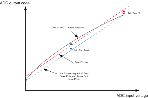
| ADC12 INL integral nonlinearity, end point(9) (See Figure 5-3) | ADC_SAMPLINGSEL = 0 to 6 for all ADC12 data | –3.9 | ±2 | 4.5 | LSB | |
| ADC12 INL integral nonlinearity, best fit(9) (See Figure 5-3) | –2.3 | ±1.5 | 2.6 | LSB | ||
| ADC12 DNL differential nonlinearity(9) | –0.8/+2.4 | LSB | ||||
| ADC Zero Scale Error | –7 | 7 | mV | |||
| ADC Full Scale Error | –35 | 35 | mV | |||
| Input bias | 2.5 V applied to pin | 400 | nA | |||
| Input leakage resistance(1) | ADC_SAMPLINGSEL= 0 or 6 | 1 | MΩ | |||
| Input Capacitance(1) | 10 | pF | ||||
| ADC single sample conversion time(1) | ADC_SAMPLINGSEL= 0 or 6 | 3.9 | μs | |||
| DIGITAL INPUTS/OUTPUTS(2)(3) | ||||||
| VOL | Low-level output voltage(4) | IOH = 4 mA, V33DIO = 3 V | DGND + 0.25 |
V | ||
| VOH | High-level output voltage (4) | IOH = –4 mA, V33DIO = 3 V | V33DIO – 0.6 | V | ||
| VIH | High-level input voltage | V33DIO = 3 V | 2.1 | V | ||
| VIL | Low-level input voltage | V33DIO = 3 V | 1.1 | V | ||
| IOH | Output sinking current | 4 | mA | |||
| IOL | Output sourcing current | –4 | mA | |||
| SYSTEM PERFORMANCE | ||||||
| TWD | Watchdog time out range | Total time is: TWD × (WDCTRL.PERIOD + 1) | 14.6 | 17 | 20.5 | ms |
| Time to disable DPWM output based on active FAULT pin signal | High level on FAULT pin | 70 | ns | |||
| Processor master clock (MCLK) | 31.25 | MHz | ||||
| tDelay | Digital compensator delay(5) | (1 clock = 32 ns) | 6 | clocks | ||
| t(reset) | Pulse width needed at reset(1) | 10 | µs | |||
| Retention period of flash content (data retention and program) | TJ = 25°C | 100 | years | |||
| Program time to erase one page or block in data flash or program flash | 20 | ms | ||||
| Program time to write one word in data flash or program flash | 20 | µs | ||||
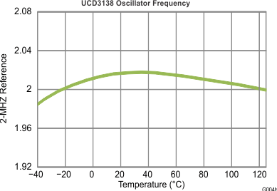
| f(PCLK) | Internal oscillator frequency | 240 | 250 | 260 | MHz | |
| Sync-in/sync-out pulse width | Sync pin | 256 | ns | |||
| Flash Read | 1 | MCLKs | ||||
| Flash Write | 20 | μs | ||||
| ISHARE | Current share current source (See Figure 6-21) | 238 | 259 | μA | ||
| RSHARE | Current share resistor (See Figure 6-21) | 9.75 | 10.3 | kΩ | ||
| POWER ON RESET AND BROWN OUT (V33D pin, See Figure 5-4) | ||||||
| VGH | Voltage good high | 2.7 | V | |||
| VGL | Voltage good low | 2.5 | V | |||
| Vres | Voltage at which IRESETsignal is valid | 0.8 | V | |||
| TPOR | Time delay after power is good or RESET relinquished | 1 | ms | |||
| Brownout | Internal signal warning of brownout conditions | 2.9 | V | |||
| TEMPERATURE SENSOR(6) | ||||||
| VTEMP | Voltage range of sensor | 1.46 | 2.44 | V | ||
| Voltage resolution | V/°C | 5.9 | mV/ºC | |||
| Temperature resolution | °C per bit | 0.1034 | ºC/LSB | |||
| Accuracy(6)(7) | –40°C to 125°C | –10 | ±5 | 10 | ºC | |
| Temperature range | –40°C to 125°C | –40 | 125 | ºC | ||
| ITEMP | Current draw of sensor when active | 30 | μA | |||
| TON | Turn on time / settling time of sensor | 100 | μs | |||
| VAMB | Ambient temperature | Trimmed 25°C reading | 1.85 | V | ||
| ANALOG COMPARATOR | ||||||
| DAC | Reference DAC Range | 0 | 2.5 | V | ||
| Reference Voltage | 2.478 | 2.5 | 2.513 | V | ||
| Bits | 7 | bits | ||||
| INL(6) | –0.42 | 0.21 | LSB | |||
| DNL(6) | 0.06 | 0.12 | LSB | |||
| Offset | –5.5 | 19.5 | mV | |||
| Time to disable DPWM output based on 0 V to 2.5 V step input on the analog comparator.(1) | 150 | ns | ||||
| Reference DAC buffered output load(8) | 0.5 | 1 | mA | |||
| Buffer offset (–0.5 mA) | 0.3 V < DAC < 2.17 V | 0 | 10 | mV | ||
| Buffer offset (1.0 mA) | 0.3 V < DAC < 2.17 V | –10 | 0 | mV | ||
5.5 Thermal Characteristics
| THERMAL METRIC(1) | UCD3138A | UCD3138A | UNIT | |
|---|---|---|---|---|
| 64 PIN QFN (RGC) |
40 PIN QFN (RMH) |
|||
| RθJA | Junction-to-ambient thermal resistance | 25.1 | 31.0 | °C/W |
| RθJC(top) | Junction-to-case (top) thermal resistance | 10.5 | 16.5 | |
| RθJB | Junction-to-board thermal resistance | 4.6 | 6.3 | |
| ψJT | Junction-to-top characterization parameter | 0.2 | 0.2 | |
| ψJB | Junction-to-board characterization parameter | 4.6 | 6.3 | |
| RθJC(bot) | Junction-to-case (bottom) thermal resistance | 1.2 | 1.1 | |
5.6 PMBus/SMBus/I2C Timing
The timing characteristics and timing diagram for the communications interface that supports I2C, SMBus, and PMBus in Slave or Master mode are shown in Section 5.6, Figure 5-1, and Figure 5-2. The numbers in Section 5.6 arµe for 400 kHz operating frequency. However, the device supports all three speeds, standard (100 kHz), fast (400 kHz). Typical values at TA = 25°C and VCC = 3.3 V (unless otherwise noted)| PARAMETER | TEST CONDITIONS | MIN | TYP | MAX | UNIT | |
|---|---|---|---|---|---|---|
| fSMB | SMBus/PMBus operating frequency | Slave mode, SMBC 50% duty cycle | 100 | 400 | kHz | |
| fI2C | I2C operating frequency | Slave mode, SCL 50% duty cycle | 100 | 400 | kHz | |
| t(BUF) | Bus free time between start and stop(1) | 1.3 | µs | |||
| t(HD:STA) | Hold time after (repeated) start(1) | 0.6 | µs | |||
| t(SU:STA) | Repeated start setup time(1) | 0.6 | µs | |||
| t(SU:STO) | Stop setup time(1) | 0.6 | µs | |||
| t(HD:DAT) | Data hold time | Receive mode | 0 | ns | ||
| t(SU:DAT) | Data setup time | 100 | ns | |||
| t(TIMEOUT) | Error signal/detect(2) | 35 | ms | |||
| t(LOW) | Clock low period | 1.3 | µs | |||
| t(HIGH) | Clock high period(3) | 0.6 | µs | |||
| t(LOW:SEXT) | Cumulative clock low slave extend time(4) | 25 | ms | |||
| tf | Clock/data fall time | Rise time tr = (VILmax – 0.15) to (VIHmin + 0.15) | 20 + 0.1 Cb(5) | 300 | ns | |
| tr | Clock/data rise time | Fall time tf = 0.9 VDD to (VILmax – 0.15) | 20 + 0.1 Cb(5) | 300 | ns | |
| Cb | Total capacitance of one bus line | 400 | pF | |||
 Figure 5-1 I2C/SMBus/PMBus Timing Diagram
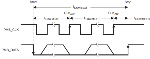 Figure 5-2 Bus Timing in Extended Mode
5.7 Parametric Measurements Information
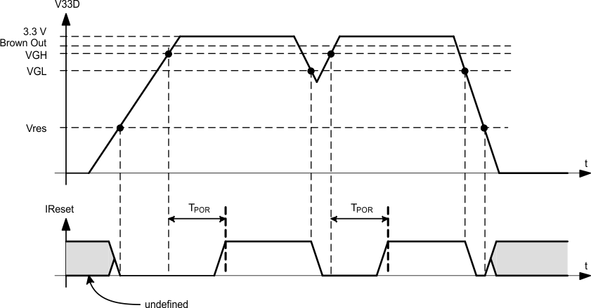 Figure 5-4 Power-On Reset (POR) and Brown-Out Reset (BOR)
| VGH | — This is the V33D threshold where the internal power is declared good. The UCD3138A comes out of reset when above this threshold. | |||
| VGL | — This is the V33D threshold where the internal power is declared bad. The device goes into reset when below this threshold. | |||
| Vres | — This is the V33D threshold where the internal reset signal is no longer valid. Below this threshold the device is in an indeterminate state. | |||
| IReset | — This is the internal reset signal. When low, the device is held in reset. This is equivalent to holding the reset pin on the IC high. | |||
| TPOR | — The time delay from when VGH is exceeded to when the device comes out of reset. | |||
| Brown out | — This is the V33D voltage threshold at which the device sets the brown out status bit. In addition an interrupt can be triggered if enabled. | |||
5.8 Peripherals
5.8.1 Digital Power Peripherals (DPPs)
At the core of the UCD3138A controller are three DDPs. Each DPP can be configured to drive from one to eight DPWM outputs. Each DPP consists of:
- Differential input error ADC (EADC) with sophisticated controls
- Hardware accelerated digital 2-pole/2-zero PID based compensator
- Digital PWM module with support for a variety of topologies
These can be connected in many different combinations, with multiple filters and DPWMs. They are capable of supporting functions like input voltage feed forward, current mode control, and constant current/constant power, and so on. The simplest configuration is shown in the following figure:

5.8.1.1 Front End
Figure 5-5 shows the block diagram of the front end module. It consists of a differential amplifier, an adjustable gain error amplifier, a high speed flash analog to digital converter (EADC), digital averaging filters and a precision high resolution set point DAC reference. The programmable gain amplifier in concert with the EADC and the adjustable digital gain on the EADC output work together to provide 9 bits of range with 6 bits of resolution on the EADC output. The output of the Front End module is a 9-bit sign extended result with a gain of 1 LSB / mV. Depending on the value of AFE selected, the resolution of this output could be either 1, 2, 4 or 8 LSBs. In addition each EADC has the ability to automatically select the AFE value such that the minimum resolution is maintained that still allows the voltage to fit within the range of the measurement. The EADC control logic receives the sample request from the DPWM module for initiating an EADC conversion. EADC control circuitry captures the EADC-9-bit-code and strobes the digital compensator for processing of the representative error. The set point DAC has 10 bits with an additional 4 bits of dithering resulting in an effective resolution of 14 bits. This DAC can be driven from a variety of sources to facilitate things like soft start, nested loops, and so on. Some additional features include the ability to change the polarity of the error measurement and an absolute value mode which automatically adds the DAC value to the error.
It is possible to operate the controller in a peak current mode control configuration; an EADC is recommended for implementing peak current mode control. In this mode, topologies like a phase shifted full bridge converter can be controlled to maintain transformer flux balance. The internal DAC can be ramped at a synchronously controlled slew rate to achieve a programmable slope compensation. This eliminates the sub-harmonic oscillation as well as improves input voltage feed-forward performance. A0 is a unity gain buffer used to isolate the peak current mode comparator. The offset of this buffer is specified in Section 5.4.
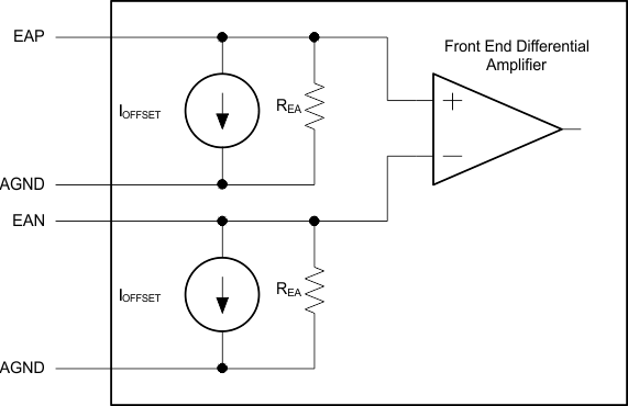 Figure 5-5 Input Stage of EADC Module
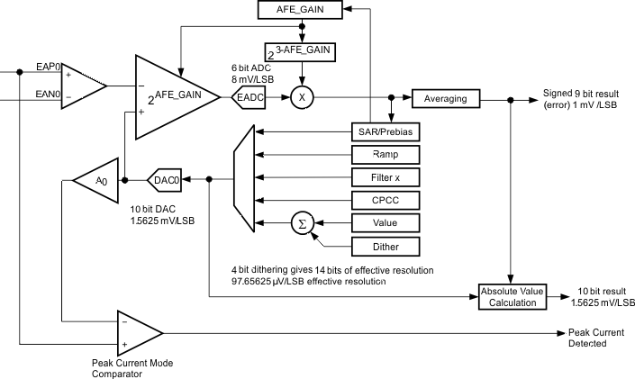 Figure 5-6 Front End Module
(Front End 2 Recommended for Peak Current Mode Control)
5.8.1.2 DPWM Module
The DPWM module represents one complete DPWM channel with 2 independent outputs, A and B. Multiple DPWM modules within the UCD3138A system can be configured to support all key power topologies. DPWM modules can be used as independent DPWM outputs, each controlling one power supply output voltage rail. It can also be used as a synchronized DPWM—with user selectable phase shift between the DPWM channels to control power supply outputs with multiphase or interleaved DPWM configurations.
The output of the filter feeds the high resolution DPWM module. The DPWM module produces the pulse width modulated outputs for the power stage switches. The compensator calculates the duty ratio as a 24-bit number in Q23 fixed point format (23 bit integer with 1 sign bit). This represents a value within the range 0.0 to 1.0. This duty ratio value is used to generate the corresponding DPWM output ON time. The resolution of the DPWM ON time is 250 psec.
Each DPWM module can be synchronized to another module or to an external sync signal. An input SYNC signal causes a DPWM ramp timer to reset. The SYNC signal outputs—from each of the four DPWM modules—occur when the ramp timer crosses a programmed threshold. In this way the phase of the DPWM outputs for multiple power stages can be tightly controlled.
The DPWM logic is probably the most complex of the Digital Peripherals. It receives the output of the compensator and converts it into the correct DPWM output for several power supply topologies. It provides for programmable dead times and cycle adjustments for current balancing between phases. It controls the triggering of the EADC. It can synchronize to other DPWMs or to external sources. It can provide synchronization information to other DPWMs or to external recipients. In addition, it interfaces to several fault handling circuits. Some of the control for these fault handling circuits is in the DPWM registers. Fault handling is covered in the Fault Mux section.
Each DPWM module supports the following features:
- Dedicated 14 bit time-base with period and frequency control
- Shadow period register for end of period updates.
- Quad-event control registers (A and B, rising and falling) (Events 1 to 4)
- Used for on/off DPWM duty ratio updates.
- Phase control relative to other DPWM modules
- Sample trigger placement for output voltage sensing at any point during the DPWM cycle.
- Support for two independent edge placement DPWM outputs (same frequency or period setting)
- Dead-time between DPWM A and B outputs
- High Resolution capabilities – 250 ps
- Pulse cycle adjustment of up to ±8.192 µs (32768 × 250 ps)
- Active high/ active low output polarity selection
- Provides events to trigger both CPU interrupts and start of ADC12 conversions.
5.8.1.3 DPWM Events
Each DPWM can control the following timing events:
- Sample Trigger Count–This register defines where the error voltage is sampled by the EADC in relationship to the DPWM period. The programmed value set in the register should be one fourth of the value calculated based on the DPWM clock. The clock controlling the circuitry runs at one fourth of the DPWM clock (PCLK = 250 MHz max). When this sample trigger count is equal to the DPWM Counter, it initiates a front end calculation by triggering the EADC, resulting in a CLA calculation, and a DPWM update. Oversampling can be set for 2, 4, or 8 times the sampling rate.
- Phase Trigger Count – count offset for slaving another DPWM (Multi-Phase/Interleaved operation).
- Period – low resolution switching period count. (count of PCLK cycles)
- Event 1 – count offset for rising DPWM A event. (PCLK cycles)
- Event 2 – DPWM count for falling DPWM A event that sets the duty ratio. Last 4 bits of the register are for high resolution control. Upper 14 bits are the number of PCLK cycle counts.
- Event 3 – DPWM count for rising DPWM B event. Last 4 bits of the register are for high resolution control. Upper 14 bits are the number of PCLK cycle counts.
- Event 4 – DPWM count for falling DPWM B event. Last 4 bits of the register are for high resolution control. Upper 14 bits are the number of PCLK cycle counts.
- Cycle Adjust – Constant offset for Event 2 and Event 4 adjustments.
Basic comparisons between the programmed registers and the DPWM counter can create the desired edge placements in the DPWM. High resolution edge capability is available on Events 2, 3, and 4.
Figure 5-7 is for multi-mode, open loop. Open loop means that the DPWM is controlled entirely by its own registers, not by the filter output. In other words, the power supply control loop is not closed.
The Sample Trigger signals are used to trigger the front end to sample input signals. The Blanking signals are used to blank fault measurements during noisy events, such as FET turn on and turn off.
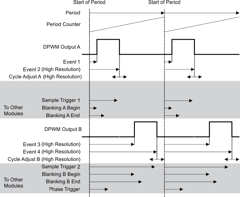
- DPWM A Rising Edge = Event 1
- DPWM A Falling Edge = Event 2 + Cycle Adjust A
- DPWM B Rising Edge = Event 3
- DPWM B Falling Edge = Event 4 + Cycle Adjust B
- Phase Trigger = Phase Trigger Register value or Filter Duty
Events always set by their registers, regardless of mode:
- Sample Trigger 1, Sample Trigger 2, Blanking A Begin, Blanking A End, Blanking B
- Begin, Blanking B End
5.8.1.4 High Resolution DPWM
Unlike conventional PWM controllers where the frequency of the clock dictates the maximum resolution of PWM edges, the UCD3138A DPWM can generate waveforms with resolutions as small as 250 ps. This is 16× the resolution of the clock driving the DPWM module.
This is achieved by providing the DPWM mechanism with 16 phase shifted clock signals of 250 MHz. The high resolution section of DPWM can be enabled or disabled, and the resolution can be defined in several steps between 4 ns to 250 ps. This is done by setting the values of PWM_HR_MULTI_OUT_EN and HIRES_SCALE inside the DPWM Control register 1. See the Power Peripherals programmer’s manual for details.
5.8.1.5 Oversampling
The DPWM module has the capability to trigger an oversampling event by initiating the EADC to sample the error voltage. The default 00 configuration has the DPWM trigger the EADC once based on the sample trigger register value. The over sampling register has the ability to trigger the sampling 2, 4 or 8 times per PWM period. Thus the time the over sample happens is at the divide by 2, 4, or 8 time set in the sampling register. The 01 setting triggers 2X oversampling, the 10 setting triggers 4X over sampling, and the 11 triggers oversampling at 8X.
5.8.1.6 DPWM Interrupt Generation
The DPWM has the capability to generate a CPU interrupt based on the PWM frequency programmed in the period register. The interrupt can be scaled by a divider ratio of up to 255 for developing a slower interrupt service execution loop. This interrupt can be fed to the ADC circuitry for providing an ADC12 trigger for sequence synchronization. Table 5-1 outlines the divide ratios that can be programmed.
5.8.1.7 DPWM Interrupt Scaling/Range
Table 5-1 DPWM Interrupt Divide Ratio
| Interrupt Divide Setting | Interrupt Divide Count | Interrupt Divide Count (hex) | Switching Period Frames (Assume 1-MHz Loop) | Number of 32-MHz Processor Cycles |
|---|---|---|---|---|
| 1 | 0 | 00 | 1 | 32 |
| 2 | 1 | 01 | 2 | 64 |
| 3 | 3 | 03 | 4 | 128 |
| 4 | 7 | 07 | 8 | 256 |
| 5 | 15 | 0F | 16 | 512 |
| 6 | 31 | 1F | 32 | 1024 |
| 7 | 47 | 2F | 48 | 1536 |
| 8 | 63 | 3F | 64 | 2048 |
| 9 | 79 | 4F | 80 | 2560 |
| 10 | 95 | 5F | 96 | 3072 |
| 11 | 127 | 7F | 128 | 4096 |
| 12 | 159 | 9F | 160 | 5120 |
| 13 | 191 | BF | 192 | 6144 |
| 14 | 223 | DF | 224 | 7168 |
| 15 | 255 | FF | 256 | 8192 |
5.8.1.8 Synchronous Rectifier Dead Time Optimization Peripheral
The UCD3138A has an advanced dead time control interface where it can accept UCD7138 output signals and optimize SR gate driver signals accordingly. The UCD7138 low-side MOSFET driver is a high-performance driver for secondary-side synchronous rectification (SR) with body diode conduction sensing. The device is suitable for high power high efficiency isolated converter applications where dead-time optimization is desired. The UCD7138 gate driver is a companion device to UCD3138A highly integrated digital controller for isolated power.
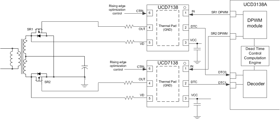 Figure 5-8 Synchronous Rectifier Peripheral use with Synchronous Rectifier Driver
DTC0 and DTC1 are received body diode conduction inputs from UCD7138. SR0_DPWM and SR1_DPWM are the DPWM waveforms for the SRs. The red and green edges are moving edges controlled by both the filter output and the DTC interface. In each cycle, right after the falling edge of the SR DPWM waveform, a body diode conduction time detection window is generated. The detection window is defined by both DETECT_BLANK and DETECT_LEN registers. During this detection window, a 4-ns timer capture counts how long the body diode conducts. Then the DPWM turn off edge of the next cycle is adjusted accordingly.
Figure 5-10 shows how the turn off edge is adjusted based on the DTC measurement of the previous cycle. The A_ADJ and B_ADJ registers in DTCMONITOR are signed accumulators; default value is 0.
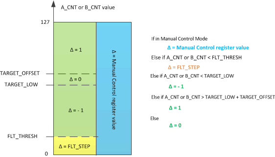 Figure 5-10 DTC Interface Principle
Based on the DTC measured, in the next cycle:
- A_ADJ = A_ADJ + A_∆
- A_ADJ = A_ADJ + B_∆
In each cycle, the A_ADJ and B_ADJ accumulator values are dynamically adjust the dead time. The ∆ value changes after the measured body diode conduction time. A_ADJ and B_ADJ have been measured and compared to the threshold values in automatic control mode. A_ADJ and B_ADJ can be controlled by firmware while in manual control mode.
Other figures of this peripheral include negative current fault protection, consecutive fault counter, DTC input multiplexor, etc. For details, refer to the programmer's manual.
5.9 Typical Temperature Characteristics
sp
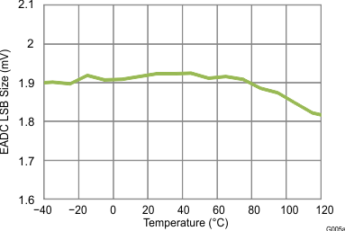 Figure 5-11 EADC LSB Size With 4X Gain (mV) vs Temperature
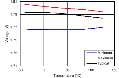
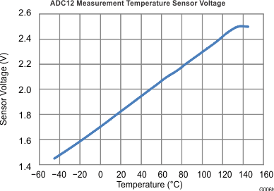 Figure 5-13 ADC12 Measurement Temperature Sensor Voltage vs Temperature
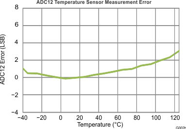 Figure 5-15 ADC12 Temperature Sensor Measurement Error vs Temperature
