ZHCSDJ8A March 2015 – April 2015 UCD3138A
PRODUCTION DATA.
- 1器件概述
- 2修订历史记录
- 3Device Comparison
- 4Terminal Configuration and Functions
- 5Specifications
-
6Detailed Description
- 6.1 Overview
- 6.2 ARM Processor
- 6.3 Memory
- 6.4 System Module
- 6.5 DPWM Modes of Operation
- 6.6 Sync FET Ramp and IDE Calculation
- 6.7 Automatic Mode Switching
- 6.8 DPWMC, Edge Generation, IntraMux
- 6.9 Filter
- 6.10 Communication Ports
- 6.11 Miscellaneous Analog
- 6.12 Package ID Information
- 6.13 Brownout
- 6.14 Global I/O
- 6.15 Temperature Sensor Control
- 6.16 I/O Mux Control
- 6.17 Current Sharing Control
- 6.18 Temperature Reference
-
7Application, Implementation, and Layout
- 7.1 Application Information
- 7.2 Typical Application
- 7.3 Layout
- 7.4 Power Supply Decoupling and Bulk Capacitors
- 8器件和文档支持
- 9机械封装和可订购信息
封装选项
机械数据 (封装 | 引脚)
散热焊盘机械数据 (封装 | 引脚)
订购信息
7 Application, Implementation, and Layout
NOTE
Information in the following applications sections is not part of the TI component specification, and TI does not warrant its accuracy or completeness. TI’s customers are responsible for determining suitability of components for their purposes. Customers should validate and test their design implementation to confirm system functionality.
7.1 Application Information
The UCD3138A has an extensive set of fully-programmable, high-performance peripherals that make it suitable for a wide range of power supply applications. In order to make the part easier to use, TI has prepared an extensive set of materials to demonstrate the features of the device for several key applications. In each case the following items are available:
- Full featured EVM hardware that demonstrates classic power supply functionality.
- An EVM user guide that contains schematics, bill-of-materials, layout guidance and test data showcasing the performance and features of the device and the hardware.
- A firmware programmers manual that provides a step-by-step walk through of the code.
Table 7-1 Application Information
| APPLICATION | EVM DESCRIPTION | |
|---|---|---|
| Phase shifted full bridge | This EVM demonstrates a PSFB DC-DC power converter with digital control using the UCD3138A device. Control is implemented by using PCMC with slope compensation. This simplifies the hardware design by eliminating the need for a series blocking capacitors and providing the inherent input voltage feed-forward that comes from PCMC. The controller is located on a daughter card and requires firmware in order to operate. This firmware, along with the entire source code, is made available through TI. A free, custom function GUI is available to help the user experiment with the different hardware and software enabled features. The EVM accepts a DC input from 350 VDC to 400 VDC, and outputs a nominal 12 VDC with full load output power of 360 W, or full output current of 30 A. | |
| LLC resonant converter |
This EVM demonstrates an LLC resonant half-bridge DC-DC power converter with digital control using the UCD3138A device. The controller is located on a daughter card and requires firmware in order to operate. This firmware, along with the entire source code, is made available through TI. A free, custom function GUI is available to help the user experiment with the different hardware and software enabled features. The EVM accepts a DC input from 350 VDC to 400 VDC, and outputs a nominal 12 VDC with full load output power of 340 W, or full output current of 29 A. |
|
7.2 Typical Application
This section summarizes the PSFB EVM DC-DC power converter.
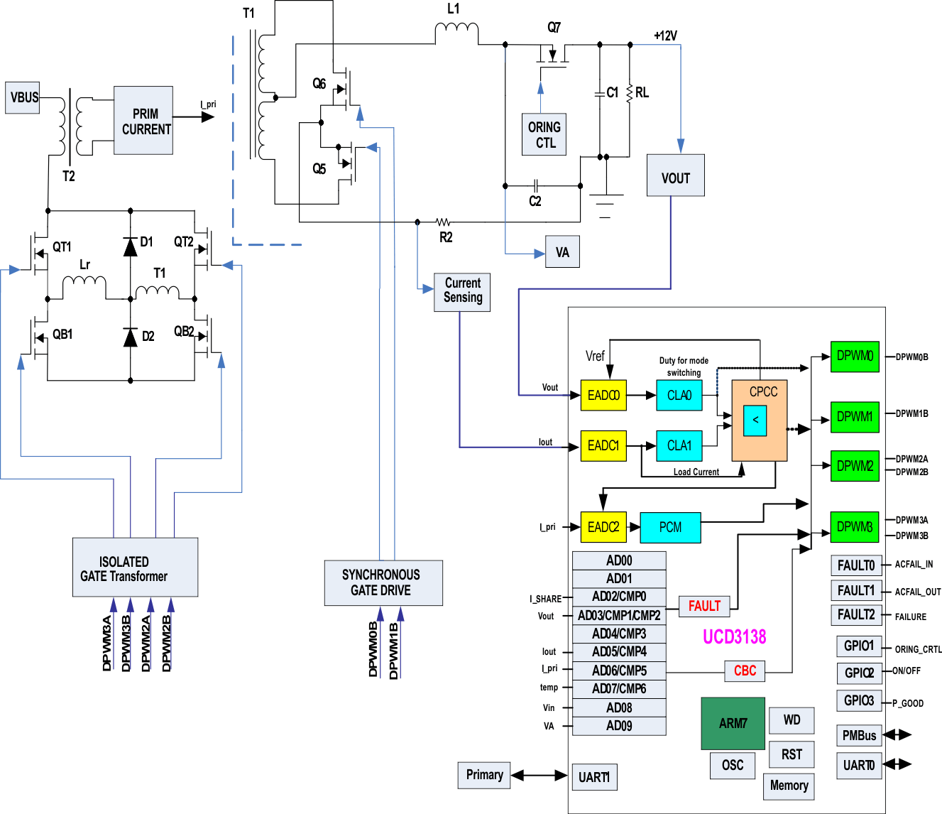 Figure 7-1 Phase-Shifted Full-Bridge
7.2.1 Design Requirements
Table 7-2 Input Characteristics
| PARAMETER | CONDITIONS | MIN | TYP | MAX | UNIT | |
|---|---|---|---|---|---|---|
| ALL SPECIFICATIONS at Vin=400V and 25°C AMBIENT UNLESS OTHERWISE NOTED. | ||||||
| Vin | Input voltage range | Normal Operating | 350 | 385 | 420 | V |
| Vinmax | Max input voltage | Continuous | 420 | V | ||
| Iin | Input current | Vin=350V, Full Load | 1.15 | A | ||
| Istby | Input no load current | Output current is 0A | 30 | mA | ||
| Von | Undervoltage lockout | Vin Decreasing (input voltage is detected on secondary side) | 340 | V | ||
| Vhys | Vin Increasing | 360 | V | |||
Table 7-3 Output Characteristics
| PARAMETER | CONDITIONS | MIN | TYP | MAX | UNIT | |
|---|---|---|---|---|---|---|
| ALL SPECIFICATIONS at Vin=400V and 25°C AMBIENT UNLESS OTHERWISE NOTED. | ||||||
| VO | Output voltage setpoint | No load on outputs | 12 | V | ||
| Regline | Line regulation | All outputs; 360 ≤ Vin ≤ 420; IO = IOmax | 0.5% | |||
| Regload | Load regulation | All outputs; 0 ≤ IO ≤ IOmax; Vin = 400 V | 1% | |||
| Vn | Ripple and noise(1) | 5 Hz to 20 MHz | 100 | mVpp | ||
| IO | Output current | 0 | 30 | A | ||
| η | Efficiency at phase-shift mode | Vo = 12 V, Io = 15 A | 93% | |||
| η | Efficiency at PWM ZVS mode | Vo = 12 V, Io = 15 A | 93% | |||
| η | Efficiency at hard switching mode | Vo = 12 V, Io = 15 A | 90% | |||
| Vadj | Output adjust range | 11.4 | 12.6 | V | ||
| Vtr | Transient response overshoot/undershoot | 50% load step at 1 AµS, min load at 2 A | ±0.36 | V | ||
| tsettling | Transient response settling time | 100 | µS | |||
| tstart | Output rise time | 10% to 90% of Vout | 50 | mS | ||
| Overshoot | At startup | 2% | ||||
| fs | Switching frequency | Over Vin and IO ranges | 150 | kHz | ||
| Ishare | Current sharing accuracy | 50% - Full load | ±5% | |||
| φ | Loop phase margin | 10% - Full load | 45 | ° | ||
| G | Loop gain margin | 10% - Full load | 10 | dB | ||
7.2.2 Detailed Design Procedure
7.2.2.1 PCMC (Peak Current Mode Control) PSFB (Phase-Shifted Full Bridge) Hardware Configuration Overview
The hardware configuration of the UCD3138A PCMC PSFB converter contains two critical elements that are highlighted in the subsequent sections.
- DPWM initialization - This section will highlight the key register settings and considerations necessary for the UCD3138A to generate the correct MOSFET waveforms for this topology. This maintains the proper phase relationship between the MOSFETs and synchronous rectifiers as well as the proper set up required to function correctly with PCMC.
- PCMC initialization - This section will discuss the register settings and hardware considerations necessary to modulate the DPWM pins with PCMC and internal slope compensation.
7.2.2.2 DPWM Initialization for PSFB
The UCD3138A DPWM peripheral provides flexibility for a wide range of topologies. The PSFB configuration utilizes the Intra-Mux and Edge Generation Modules of the DPWM. For a diagram showing these modules, see the UCD3138A Digital Power Peripherals Manual.
Here is a schematic of the power stage of the PSFB:
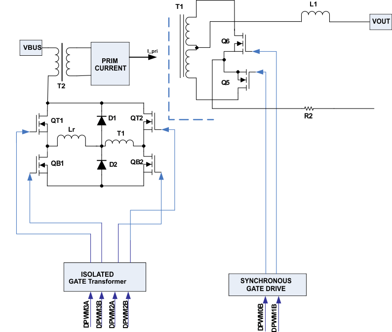 Figure 7-2 Schematic – PSFB Power Stage
Here is an overview of the key PSFB signals:
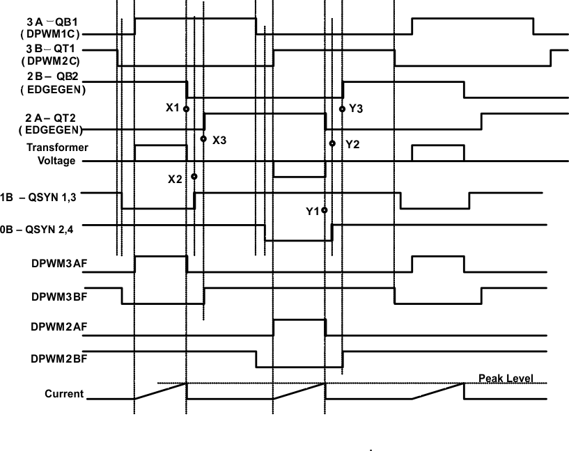
7.2.3 DPWM Synchronization
DPWM1 is synchronized to DPWM0, DPWM2 is synchronized to DPWM1, and DPWM3 is synchronized to DPWM2, ½ period out of phase using these commands:
| Dpwm1Regs.DPWMCTRL0.bit.MSYNC_SLAVE_EN = 1; //configured to slave
Dpwm2Regs.DPWMCTRL0.bit.MSYNC_SLAVE_EN = 1; // configured to slave Dpwm3Regs.DPWMCTRL0.bit.MSYNC_SLAVE_EN = 1; // configured to slave |
||
| Dpwm0Regs.DPWMPHASETRIG.all = PWM_SLAVESYNC;
Dpwm1Regs.DPWMPHASETRIG.all = PWM_SLAVESYNC; Dpwm2Regs.DPWMPHASETRIG.all = PWM_SLAVESYNC; |
||
| LoopMuxRegs.DPWMMUX.bit.DPWM1_SYNC_SEL = 0;
LoopMuxRegs.DPWMMUX.bit.DPWM2_SYNC_SEL = 1; LoopMuxRegs.DPWMMUX.bit.DPWM3_SYNC_SEL = 2; |
// Slave to dpwm-0
// Slave to dpwm-1 // Slave to dpwm-2 |
|
If the event registers on the DPWMs are the same, the two pairs of signals will be symmetrical. All code examples are taken from the PSFB EVM code, unless otherwise stated.
7.2.4 Fixed Signals to Bridge
The two top signals in the above drawing have fixed timing. The DPWM1CF and DPWM2CF signals are used for these pins. DPWMCxF refers to the signal coming out of the fault module of DPWMx, as shown in Figure 7-4.
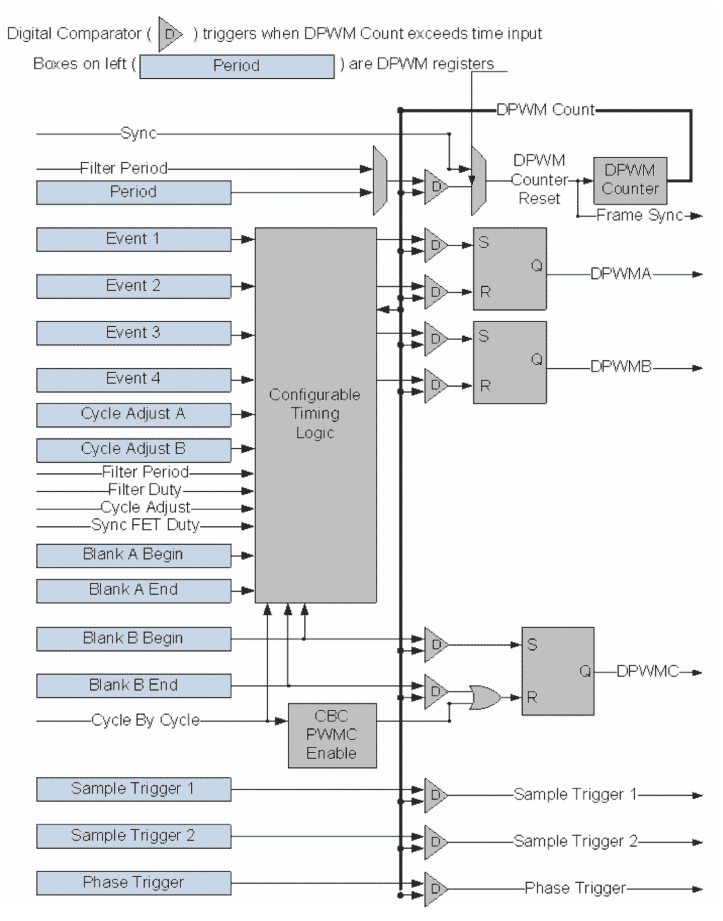 Figure 7-4 Fixed Signals to Bridge
These signals are actually routed to pins DPWM3A and 3B using the Intra Mux with these statements:
| Dpwm3Regs.DPWMCTRL0.bit.PWM_A_INTRA_MUX = 7; // Send DPWM1C
Dpwm3Regs.DPWMCTRL0.bit.PWM_B_INTRA_MUX = 8; // Send DPWM2C |
||
Since these signals are really being used as events in the timer, the #defines are called EV5 and EV6. Here are the statements which initialize them:
| // Setup waveform for DPWM-C (re-using blanking B regs)
Dpwm2Regs.DPWMBLKBBEG.all = PWM2_EV5 + (4 *16); Dpwm2Regs.DPWMBLKBEND.all = PWM2_EV6; |
||
 Figure 7-5 Blank B Timing Information
The statements for DPWM1 are the same. Remember that DPWMC reuses the Blank B registers for timing information.
7.2.5 Dynamic Signals to Bridge
DPWM0 and 1 are set at normal mode. PCMC triggering signal (fault) chops DPWM0A and 1A cycle by cycle. The corresponding DPWM0B and 1B are used for synchronous rectifier MOSFET control. The same PCMC triggering signal is applied to DPWM2 and DPWM3. Both of these are set to normal mode as well. DPWM2 and 3 are chopped and their edges are used to generate the next two dynamic signals to the bridge. They are generated using the Edge Generator Module in DPWM2. The Edge Generator sources are DPWM2 and DPWM3. The edges used are:
| DPWM2A turned on by a rising edge on DPWM2BF DPWM2A turned off by a falling edge on DPWM3AF DPWM2B turned on by a rising edge on DPWM3BF DPWM2B turned off by a falling edge on DPWM2AF |
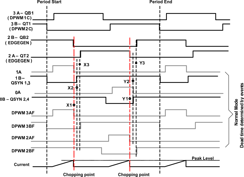
The Edge Generator is configured with these statements:
| Dpwm2Regs.DPWMEDGEGEN.bit.A_ON_EDGE = 2;
Dpwm2Regs.DPWMEDGEGEN.bit.A_OFF_EDGE = 5; Dpwm2Regs.DPWMEDGEGEN.bit.B_ON_EDGE = 6; Dpwm2Regs.DPWMEDGEGEN.bit.B_OFF_EDGE = 1; |
|
| Dpwm2Regs.DPWMCTRL0.bit.PWM_A_INTRA_MUX = 1; // EDGEGEN-A out the A output
Dpwm2Regs.DPWMCTRL0.bit.PWM_B_INTRA_MUX = 1; // EDGEGEN-B out the B output |
|
| Dpwm2Regs.DPWMEDGEGEN.bit.EDGE_EN = 1; |
The EDGE_EN bits are set for all 4 DPWMs. This is done to ensure that all signals have the same timing delay through the DPWM.
The finial 6 gate signals are shown in Figure 7-7.
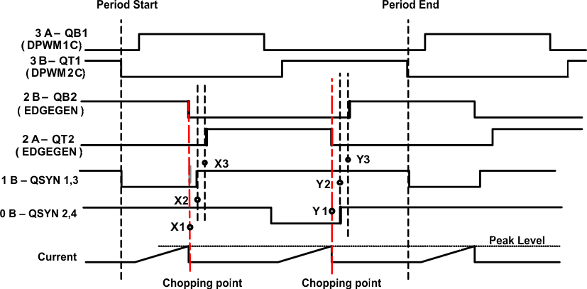 Figure 7-7 Final 6 Gate Signals
Note how the falling edge of DPWM2AF aligns with the X1 edge, and how the rising edge of DPWM2BF aligns with the X3 edge. The falling edges on DPWM2AF and DPWM3AF are caused by the peak detection logic. This is fed through the Cycle By Cycle logic. The Cycle By Cycle logic also has a special feature to control the rising edges of DPWM2BF (X1 and X3) and DPWM3BF (Y1 and Y3). It uses the value of Event3 – Event2 to control the time between the edges. The same feature is used with DPWM0 and DPWM1 to control the X2 and Y2 signals. Using the other 2 DPWMs permits these signals to have a different dead time.
The same setup can be used for voltage mode control. In this case, the Filter output sets the timing of the falling edge on DPWMxAF.
All DPWMs are configured in Normal mode, with CBC enabled. If external slope compensation is used, DPWM1A and DPWM1B are used to reset the external compensator at the beginning of each half cycle. If no PCMC event occurs, the values of Events 2 and 3 determine the locations of the edges, just as in open loop mode.
7.2.6 System Initialization for PCM
PCM (Peak Current Mode) is a specialized configuration for the UCD3138A which involves several peripherals. This section describes how it works across the peripherals.
7.2.6.1 Use of Front Ends and Filters in PSFB
All three front ends are used in PSFB. The same signals are used in the same places for both PCMC and voltage mode. The same hardware can be used for both control modes, with the mode determined by which firmware is loaded into the device. FE0 and FE1 are used with their associated filters, but Filter 2 is not used at all.
FE0 – Vout – voltage loop
FE1 – Iout – current loop
FE2 – Ipri – PCM
In PCMC mode, FE2 is used for PCMC, and the voltage loop is normally used to provide the start point for the compensation ramp. If the CPCC firmware detects a need for constant current mode, it switches to the current loop for the start point.
7.2.6.2 Peak Current Detection
Peak current detection involves all the major modules of the DPPs, the Front End, Filter, Loop Mux, Fault Mux and the DPWMs. A drawing of the major elements is shown in Figure 7-8.
 Figure 7-8 Peak Current Detection Function
The voltage loop is used to select a peak current level. This level is fed to the Ramp module to generate a compensation ramp. The compensation ramp is compared to the primary current by the PCMC comparator in the Front End. When the ramp value is greater than the primary current, the APCMC signal is sent to the DPWM, causing the events described in the previous sections.
The DPWM frame start and output pin signals can be used to trigger the Ramp Module. In this case, each DPWM frame triggers the start of the ramp. The ramp steps every 32 ns.
The PCM_FILTER_SEL bits in the LoopMux.PCMCTRL register are used to select which filter is connected to the ramp module:
LoopMuxRegs.PCMCTRL.bit.PCM_FILTER_SEL =0; //select filter0
With Firmware Constant Power/Constant current, Filter 1 and Front End 1 are used as a current control loop, with the EADCDAC set to high current. If the voltage loop value becomes higher than the current loop value, then Filter 1 is used to control the PCM ramp start value:
LoopMuxRegs.PCMCTRL.bit.PCM_FILTER_SEL =1;
S P A C E //select filter1 for slope compensation source
In the ramp module, there are 2 bitfields in the RAMPCTRL register which must be configured. The PCM_START_SEL must be set to a 1 to enable the Filter to be used as a ramp start source. The RAMP_EN bit must be set, of course.
The DAC_STEP register sets the slope of the compensation ramp. The DAC value is in volts, of course, so it is necessary to calculate the slope after the current to voltage conversion. Here is the formula for converting from millivolts per microsecond to DACSTEP.
m = compensation slope in millivolts per microsecond
ACSTEP = 335.5 × M
In C, this can be written:
| #define COMPENSATION_SLOPE 150 //compensation slope in millivolts per microsecond
#define DACSTEP_COMP_VALUE ((int) (COMPENSATION_SLOPE*335.5) ) S P A C E //value in DACSTEP for desired compensation slope |
|
| S P A C E FeCtrl0Regs.DACSTEP.all = DACSTEP_COMP_VALUE; | |
It may also be necessary to set a ramp ending value in the RAMPDACEND register.
In addition, it is necessary to set the D2S_COMP_EN bit in the EADCCTRL register. This is for enabling the differential to single ended comparator function. The front end diagram leaves it out for simplicity, but the connection between the DAC and the EADC amplifier is actually differential. The PCMC comparator, however, is single ended. So a conversion is necessary as shown in Figure 7-9.
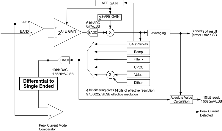 Figure 7-9 Differential to Single-Ended Comparator Function
The EADC_MODE bit in EADCCTRL should be set to a 5 for peak current mode.
The peak current detection signal next goes to the Loop Mux. The Fault Mux has only 1 APCM input, but there are 3 front ends. So the PCM_FE_SEL bits in APCMCTRL must be used to select which front end is used:
LoopMuxRegs.APCMCTRL.bit.PCM_FE_SEL = 2; // use FE2 for PCM */
The PCM_EN bit must also be set.
LoopMuxRegs.APCMCTRL.bit.PCM_EN = 1; // Enable PCM
Next the Fault Mux is used to enable the APCM bit to the CLIM/CBC signal to the DPWM. There are 4 DPWMxCLIM registers, one for each DPWM. The ANALOG_PCM_EN bit must be set in each one to connect the PCM detection signal to the CLIM/CBC signal on each DPWM. For the latest configuration information on all of these bits, consult the appropriate EVM firmware. To avoid errors, it is best to configure your hardware design using the same DPWMs, filters, and front ends for the same functions as the EVM.
DPWM timing is used to trigger the start of the ramp. This is selected by the FECTRLxMUX registers in the Loop Mux. DPWMx_FRAME_SYNC_EN bits, when set, cause the ramp to be triggered at the start of the DPWM period.
7.2.6.3 Peak Current Mode (PCM)
There is one peak current mode control module in the device however any front end can be configured to use this module.
7.2.7 Application Performance Plots
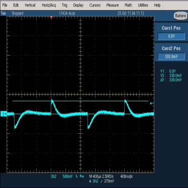
| 1A-16A-1A | Vin =385V |
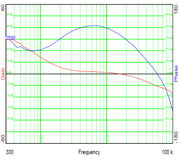
| Kp =14000 Ki =300 |
Kd =2000 | |
| Alpha = –2 |
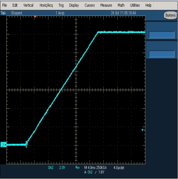
| 30A Load | syncFETs off |
7.3 Layout
7.3.1 Layout Guidelines
- Single ground is recommended: SGND. A multilayer such as 4 layers board is recommended so that one solid SGND is dedicated for return current path, referred to the layout example.
- Apply multiple different capacitors for different frequency range on decoupling circuits. Each capacitor has different ESL, Capacitance and ESR, and they have different frequency response.
- Avoid long traces close to radiation components, and place them into an internal layer, and it is preferred to have grounding shield, and in the end, add a termination circuit;
- Analog circuit such as ADC sensing lines needs a return current path into the analog circuitry; digital circuit such as GPIO, PMBus and PWM has a return current path into the digital circuitry; although with a single plane, still try to avoid to mix analog current and digital current.
- Don’t use a ferrite bead or larger than 3 Ω resistor to connect between V33A and V33D.
- Both 3.3VD and 3.3VA should have local 4.7 µF decoupling capacitors close to the device power pins, add visas to connect decoupling caps directly to SGND.
- Avoid negative current/negative voltage on all pins, so Schottky diodes may need to clamp the voltage; avoid the voltage spike on all pins more than 3.8 V or less than –0.3 V, add Schottky diodes on the pins which could have voltage spikes during surge test; be aware that a Schottky has relatively higher leakage current, which can affect the voltage sensing at high temperature.
- RESET pin should have one at least 2.2 µF low ESL capacitor locally decoupled with SGND plane. This capacitor must be located close to the device RESET pin. It is highly recommended to use a small resistance (such as 220 Ω) to connect the RESET pin with 3.3 VD.
7.3.2 Layout Example
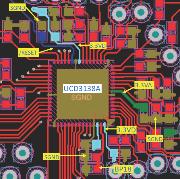 Figure 7-13 UCD3138A Layout Example
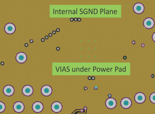 Figure 7-14 UCD3138A Layout Example, Internal Plane
7.4 Power Supply Decoupling and Bulk Capacitors
- Both 3.3 VD and 3.3 VA should have a local 4.7-μF capacitor placed as close as possible to the device pins.
- BP18 should have a 1-μF capacitor.