ZHCSDN7B March 2015 – May 2015 UCD7138
PRODUCTION DATA.
- 1 特性
- 2 应用
- 3 说明
- 4 简化电路原理图
- 5 修订历史记录
- 6 Pin Configuration and Functions
- 7 Specifications
- 8 Detailed Description
- 9 Application and Implementation
- 10Power Supply Recommendations
- 11Layout
- 12器件和文档支持
- 13机械、封装和可订购信息
11 Layout
11.1 Layout Guidelines
Proper PCB layout is extremely important in a high-current, fast-switching circuit to provide appropriate device operation and design robustness. The following circuit layout guidelines are strongly recommended.
- Place the driver device as close as possible to power and ground to minimize the length of high-current traces between the output pins and the gate of the power device.
- Place the VCC bypass capacitors between the VCC pin and ground as close as possible to the driver with minimal trace length to improve the noise filtering. These capacitors support the high-peak current that is drawn from the VCC supply during turnon of the power MOSFET. The use of low inductance SM components such as chip resistors and chip capacitors is highly recommended.
- The turnon and turnoff current-loop paths (driver device, power MOSFET, and VCC bypass capacitors) should be minimized as much as possible to keep the stray inductance to a minimum.
- Separate power traces and signal traces, such as output and input signals.
- Star-point grounding is a good way to minimize noise coupling from one current loop to another. The ground of the driver should be connected to the other circuit nodes such as the source of power switch, ground of PWM controller, and others at one single point. The connected paths should be as short as possible and as wide as possible to reduce resistance and inductance.
- Use a ground plane to provide noise shielding. Fast rise and fall times at the OUT pin can corrupt the input signals during transition. The ground plane must not be a conduction path for any current loop. Instead, the ground plane must be connected to the star-point with one single trace to establish the ground potential.
- A 1-Ω resistor may be connected between OUT pin and the gate terminal of the MOSFET to reduce gate to source voltage ringing.
- A 20-Ω resistor should be connected between VD pin and the drain terminal of the MOSFET to limit the current flowing out of VD pin when the drain terminal voltage is negative.
11.2 Layout Example
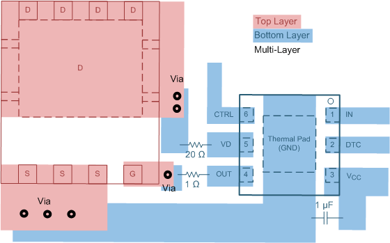
 Figure 45. Layout Example With Surface-Mount MOSFET
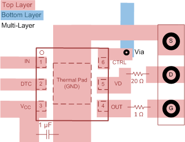
 Figure 46. Layout Example With Through-Hole MOSFET