ZHCS212C April 2011 – March 2019 UCD90120A
PRODUCTION DATA.
- 1 特性
- 2 应用
- 3 说明
- 4 修订历史记录
- 5 Pin Configuration and Functions
- 6 Specifications
-
7 Detailed Description
- 7.1 Overview
- 7.2 Functional Block Diagram
- 7.3 Feature Description
- 7.4
Device Functional Modes
- 7.4.1 Power-Supply Sequencing
- 7.4.2 Pin-Selected Rail States
- 7.4.3 Monitoring
- 7.4.4 Fault Responses and Alert Processing
- 7.4.5 Shut Down All Rails and Sequence On (Resequence)
- 7.4.6 GPIOs
- 7.4.7 GPO Control
- 7.4.8 GPO Dependencies
- 7.4.9 GPO Delays
- 7.4.10 State Machine Mode Enable
- 7.4.11 GPI Special Functions
- 7.4.12 Power-Supply Enables
- 7.4.13 Cascading Multiple Devices
- 7.4.14 PWM Outputs
- 7.4.15 Programmable Multiphase PWMs
- 7.4.16 Margining
- 7.4.17 System Reset Signal
- 7.4.18 Watch Dog Timer
- 7.4.19 Run Time Clock
- 7.4.20 Data and Error Logging to Flash Memory
- 7.4.21 Brownout Function
- 7.4.22 PMBus Address Selection
- 7.5 Programming
- 8 Application and Implementation
- 9 Power Supply Recommendations
- 10Layout
- 11器件和文档支持
- 12机械、封装和可订购信息
7.4.9 GPO Delays
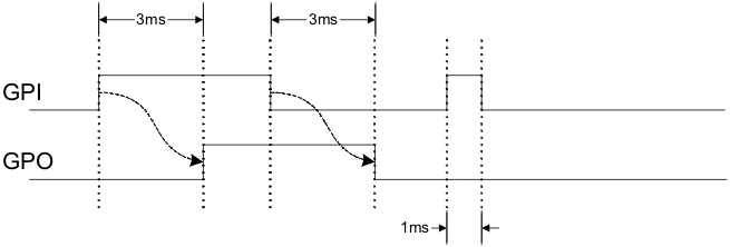
The GPOs can be configured so that they manifest a change in logic with a delay on assertion, deassertion, both or none. GPO behavior using delays will have different effects depending if the logic change occurs at a faster rate than the delay. On a normal delay configuration, if the logic for a GPO changes to a state and reverts back to previous state within the time of a delay then the GPO will not manifest the change of state on the pin. In Figure 20 the GPO is set so that it follows the GPI with a 3ms delay at assertion and also at de-assertion. When the GPI first changes to high logic state, the state is maintained for a time longer than the delay allowing the GPO to follow with appropriate logic state. The same goes for when the GPI returns to its previous low logic state. The second time that the GPI changes to a high logic state it retuns to low logic state before the delay time expires. In this case the GPO does not change state. A delay configured in this manner serves as a glitch filter for the GPO.
 Figure 20. GPO Behavior When Not Ignoring Inputs During Delay
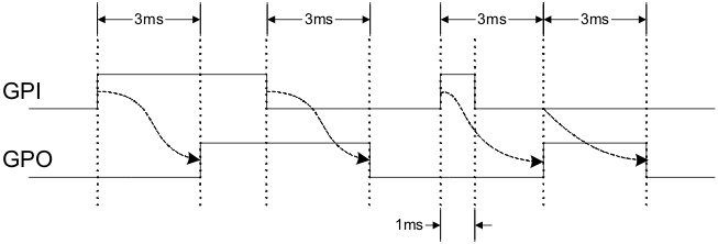
 The Ignore Input During Delay bit allows to output a change in GPO even if it occurs for a time shorter than the delay. This configuration setting has the GPO ignore any activity from the triggering event until the delay expires. Figure 21 represents the two cases for when ignoring the inputs during a delay. In the case in which the logic changes occur with more time than the delay, the GPO signal looks the same as if the input was not ignored. Then on a GPI pulse shorter than the delay the GPO still changes state. Any pulse that occurs on the GPO when having the Ignore Input During Delay bit set will have a width of at least the time delay.
 Figure 21. GPO Behavior When Ignoring Inputs During Delay