ZHCSJQ1D November 2010 – April 2019 UCD90160
PRODUCTION DATA.
- 1 特性
- 2 应用
- 3 说明
- 4 修订历史记录
- 5 Pin Configuration and Functions
- 6 Specifications
-
7 Detailed Description
- 7.1 Overview
- 7.2 Functional Block Diagram
- 7.3 Feature Description
- 7.4
Device Functional Modes
- 7.4.1 Power-Supply Sequencing
- 7.4.2 Pin-Selected Rail States
- 7.4.3 Voltage Monitoring
- 7.4.4 Fault Responses and Alert Processing
- 7.4.5 Shut Down All Rails and Sequence On (Resequence)
- 7.4.6 GPIOs
- 7.4.7 GPO Control
- 7.4.8 GPO Dependencies
- 7.4.9 GPI Special Functions
- 7.4.10 Power-Supply Enables
- 7.4.11 Cascading Multiple Devices
- 7.4.12 PWM Outputs
- 7.4.13 Programmable Multiphase PWMs
- 7.4.14 Margining
- 7.4.15 System Reset Signal
- 7.4.16 Watch Dog Timer
- 7.4.17 Run Time Clock
- 7.4.18 Data and Error Logging to Flash Memory
- 7.4.19 Brownout Function
- 7.4.20 PMBus Address Selection
- 7.5 Programming
- 8 Application and Implementation
- 9 Power Supply Recommendations
- 10Layout
- 11器件和文档支持
- 12机械、封装和可订购信息
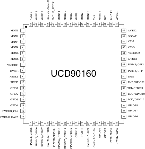
5 Pin Configuration and Functions
RGC Package with Thermal Pad
64-Pin VQFN
Top View


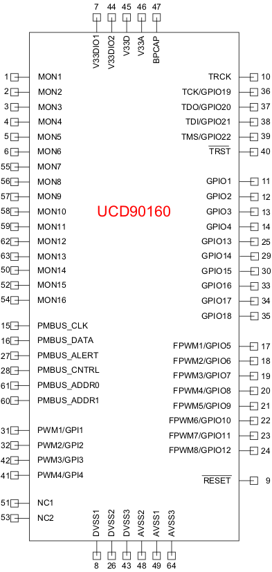
Pin Functions(1)
| PIN | I/O | DESCRIPTION | |
|---|---|---|---|
| NAME | NO. | ||
| ANALOG MONITOR INPUTS | |||
| MON1 | 1 | I | Analog input (0 V–2.5 V) |
| MON2 | 2 | I | Analog input (0 V–2.5 V) |
| MON3 | 3 | I | Analog input (0 V–2.5 V) |
| MON4 | 4 | I | Analog input (0 V–2.5 V) |
| MON5 | 5 | I | Analog input (0 V–2.5 V) |
| MON6 | 6 | I | Analog input (0 V–2.5 V) |
| MON7 | 55 | I | Analog input (0 V–2.5 V) |
| MON8 | 56 | I | Analog input (0 V–2.5 V) |
| MON9 | 57 | I | Analog input (0 V–2.5 V) |
| MON10 | 58 | I | Analog input (0 V–2.5 V) |
| MON11 | 59 | I | Analog input (0 V–2.5 V) |
| MON12 | 62 | I | Analog input (0 V–2.5 V) |
| MON13 | 63 | I | Analog input (0 V–2.5 V) |
| MON14 | 50 | I | Analog input (0.2 V–2.5 V) |
| MON15 | 52 | I | Analog input (0.2 V–2.5 V) |
| MON16 | 54 | I | Analog input (0.2 V–2.5 V) |
| GENERAL-PURPOSE INPUT AND OUTPUT | |||
| GPIO1 | 11 | I/O | General-purpose discrete I/O |
| GPIO2 | 12 | I/O | General-purpose discrete I/O |
| GPIO3 | 13 | I/O | General-purpose discrete I/O |
| GPIO4 | 14 | I/O | General-purpose discrete I/O |
| GPIO13 | 25 | I/O | General-purpose discrete I/O |
| GPIO14 | 29 | I/O | General-purpose discrete I/O |
| GPIO15 | 30 | I/O | General-purpose discrete I/O |
| GPIO16 | 33 | I/O | General-purpose discrete I/O |
| GPIO17 | 34 | I/O | General-purpose discrete I/O |
| GPIO18 | 35 | I/O | General-purpose discrete I/O |
| PWM OUTPUTS | |||
| FPWM1/GPIO5 | 17 | I/O/PWM | PWM (15.259 kHz to 125 MHz) or GPIO |
| FPWM2/GPIO6 | 18 | I/O/PWM | PWM (15.259 kHz to 125 MHz) or GPIO |
| FPWM3/GPIO7 | 19 | I/O/PWM | PWM (15.259 kHz to 125 MHz) or GPIO |
| FPWM4/GPIO8 | 20 | I/O/PWM | PWM (15.259 kHz to 125 MHz) or GPIO |
| FPWM5/GPIO9 | 21 | I/O/PWM | PWM (15.259 kHz to 125 MHz) or GPIO |
| FPWM6/GPIO10 | 22 | I/O/PWM | PWM (15.259 kHz to 125 MHz) or GPIO |
| FPWM7/GPIO11 | 23 | I/O/PWM | PWM (15.259 kHz to 125 MHz) or GPIO |
| FPWM8/GPIO12 | 24 | I/O/PWM | PWM (15.259 kHz to 125 MHz) or GPIO |
| PWM1/GPI1 | 31 | I/PWM | Fixed 10-kHz PWM output or GPI |
| PWM2/GPI2 | 32 | I/PWM | Fixed 1-kHz PWM output or GPI |
| PWM3/GPI3 | 42 | I/PWM | PWM (0.93 Hz to 7.8125 MHz) or GPI |
| PWM4/GPI4 | 41 | I/PWM | PWM (0.93 Hz to 7.8125 MHz) or GPI |
| PMBus COMM INTERFACE | |||
| PMBUS_CLK | 15 | I/O | PMBus clock (must have pullup to 3.3 V) |
| PMBUS_DATA | 16 | I/O | PMBus data (must have pullup to 3.3 V) |
| PMBALERT | 27 | O | PMBus alert, active-low, open-drain output (must have pullup to 3.3 V) |
| PMBUS_CNTRL | 28 | I | PMBus control |
| PMBUS_ADDR0 | 61 | I | PMBus analog address input. Least-significant address bit |
| PMBUS_ADDR1 | 60 | I | PMBus analog address input. Most-significant address bit |
| JTAG | |||
| TRCK | 10 | O | Test return clock |
| TCK/GPIO19 | 36 | I/O | Test clock or GPIO |
| TDO/GPIO20 | 37 | I/O | Test data out or GPIO |
| TDI/GPIO21 | 38 | I/O | Test data in (tie to VDD with 10-kΩ resistor) or GPIO |
| TMS/GPIO22 | 39 | I/O | Test mode select (tie to VDD with 10-kΩ resistor) or GPIO |
| TRST | 40 | I | Test reset. Tie to ground with 10-kΩ resistor |
| INPUT POWER AND GROUNDS | |||
| RESET | 9 | Active-low device reset input. Hold low for at least 2 μs to reset the device. Refer to the Device Reset section. | |
| V33A | 46 | Analog 3.3-V supply. Refer to the Layout Guidelines section. | |
| V33D | 45 | Digital core 3.3-V supply. Refer to the Layout Guidelines section. | |
| V33DIO1 | 7 | Digital I/O 3.3-V supply. Refer to the Layout Guidelines section. | |
| V33DIO2 | 44 | Digital I/O 3.3-V supply. Refer to the Layout Guidelines section. | |
| BPCap | 47 | 1.8-V bypass capacitor. Refer to the Layout Guidelines section. | |
| AVSS1 | 49 | Analog ground | |
| AVSS2 | 48 | Analog ground | |
| AVSS3 | 64 | Analog ground | |
| DVSS1 | 8 | Digital ground | |
| DVSS2 | 26 | Digital ground | |
| DVSS3 | 43 | Digital ground | |
| QFP ground pad | NA | Thermal pad – tie to ground plane. | |
(1) The maximum number of configurable rails is 16. The maximum number of configurable GPIs is 8. The maximum number of configurable Boolean Logic GPOs is 16.