ZHCSDF1 February 2015 UCD90240
PRODUCTION DATA.
- 1 特性
- 2 应用
- 3 说明
- 4 修订历史记录
- 5 Pin Configuration and Functions
- 6 Specifications
-
7 Detailed Description
- 7.1 Device Overview
- 7.2 Functional Block Diagram
- 7.3
Feature Description
- 7.3.1 TI Fusion GUI
- 7.3.2 PMBUS Interface
- 7.3.3 Rail Setup
- 7.3.4 Rail Monitoring Configuration
- 7.3.5 GPI Configuration
- 7.3.6 Rail Sequence Configuration
- 7.3.7 Fault Responses Configuration
- 7.3.8 GPO Configuration
- 7.3.9 Margining Configuration
- 7.3.10 Pin Selected Rail States Configuration
- 7.3.11 Watchdog Timer
- 7.3.12 System Reset Function
- 7.3.13 Cascading Multiple Devices
- 7.3.14 Voltage Monitoring
- 7.3.15 Status Monitoring
- 7.3.16 Data and Error Logging to EEPROM Memory
- 7.3.17 Black Box First Fault Logging
- 7.3.18 PMBUS Address Selection
- 7.3.19 ADC Reference
- 7.3.20 Device Reset
- 7.3.21 Brownout
- 7.3.22 Device Configuration and Programming
- 7.3.23 Internal Fault Management
- 8 Application and Implementation
- 9 Power Supply Recommendations
- 10Layout
- 11器件和文档支持
- 12机械封装和可订购信息
7 Detailed Description
7.1 Device Overview
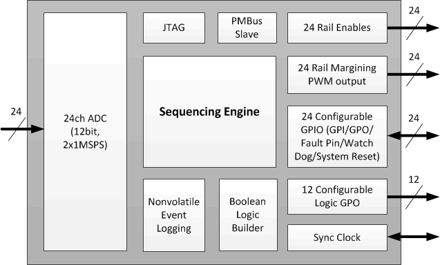
Electronic systems that include CPU, DSP, microcontroller, FPGA, ASIC, etc. can have multiple voltage rails and require certain power on/off sequences in order to function correctly. The UCD90240 can control up to 24 voltage rails and ensure correct power sequences during normal condition and fault conditions.
In addition to sequencing, UCD90240 can continuously monitor rail voltages, currents, temperatures, fault conditions, and report the system health information to upper computers through PMBus, improving systems’ long term reliability.
Also, UCD90240 can protect electronic systems by responding to power system faults. The fault responses are conveniently configured by users through Fusion GUI. Fault events are stored in on-chip nonvolatile flash memory in order to assist failure analysis. A Black Box Fault Log feature stores comprehensive system statuses at the moment when the first fault occurs. With this feature, failure analysis can be more effective.
System reliability can be improved through four-corner testing during system verification. During four-corner testing, each voltage rail is required to operate at the minimum and maximum output voltages, commonly known as margining. UCD90240 can perform accurate closed-loop margining for up to 24 voltage rails. During normal operation, UCD90240 can also actively trim DC output voltages using the same margining circuitry. This feature allows tuning rail voltages to an optimal level.
UCD90240 supports both PMBus- and pin-based control environments. UCD90240 functions as a PMBus slave. It can communicate with upper computers with PMBus commands, and control voltage rails accordingly. In addition to rail enable (EN) pins, up to 24 GPIO pins can be configured as GPOs and directly controlled by PMBus commands. Also, UCD90240 can be controlled by up to 24 GPIO configured GPI pins. The GPIs can be used as fault inputs which can shut down rails. The GPIs can be also used as Boolean logic input to control the 12 Logic GPO outputs. Each of the 12 dedicated Logic GPO pins has a flexible Boolean logic builder. Input signals of the Boolean logic builder can include GPIs, other GPOs, and selectable system flags such as POWER_GOOD, faults, warnings, etc. A simple state machine is also available for each Logic GPO pin.
UCD90240 provides additional features such as cascading, pin-selected states, system watchdog, system reset, runtime clock, peak value log, reset counter, and so on. Cascading feature offers convenient ways to cascade up to four UCD90240 devices and manage up to 96 voltage rails via one Sync Clock pin connection. Pin-selected states feature allows users to define up to 8 rail states. These states can implement system low-power modes as set out in the Advanced Configuration and Power Interface (ACPI) specification. Other UCD90240 features will be introduced in the following sections of this data sheet.
7.2 Functional Block Diagram
7.3 Feature Description
7.3.1 TI Fusion GUI
The Texas Instruments Fusion Digital Power Designer is provided for device configuration. This PC-based graphical user interface (GUI) offers an intuitive I2C/PMBus interface to the device. It allows the design engineer to configure the system operating parameters for the application without directly using PMBus commands, store the configuration to on-chip nonvolatile memory, and observe system status (voltage, current, temperature, faults, etc.). Fusion Digital Power Designer is referenced throughout the data sheet as Fusion GUI and many sections include screenshots. The Fusion GUI can be downloaded from www.ti.com. After the device has been configured, UCD90240 can perform all designed functions independently without Fusion GUI.
7.3.2 PMBUS Interface
The PMBus is a serial interface specifically designed to support power management. It is based on the SMBus interface that is built on the I2C physical specification. The UCD90240 supports revision 1.2 of the PMBus standard. Wherever possible, standard PMBus commands are used to support the function of the device. For unique features of the UCD90240, MFR_SPECIFIC commands are defined to configure or activate those features. These commands are defined in the UCD90xxx Sequencer and System Health Controller PMBUS Command Reference (SLVU352). The most current UCD90xxx PMBus™ Command Reference can be found within the TI Fusion Digital Power Designer software via the Help Menu (Help, Documentation and Help Center, Sequencers tab, Documentation section).
This document makes frequent mention of the PMBus specification. Specifically, this document is PMBus Power System Management Protocol Specification Part II – Command Language, Revision 1.2, dated 6 September 2010. The specification is published by the Power Management Bus Implementers Forum and is available from www.pmbus.org.
The UCD90240 is PMBus compliant, in accordance with the Compliance section of the PMBus specification. The firmware is also compliant with the SMBus 1.1 specification, including support for the SMBus ALERT function. The hardware can support either 100-kHz or 400-kHz PMBus operation.
7.3.3 Rail Setup
Power rails are defined under the Pin Assignment tab, as shown in Figure 1. Click corresponding buttons to add or delete a rail. After a rail is added, MON, EN, and MARGIN pins can be assigned to the rail. UCD90240 has 24 MON pins, 24 EN pin, and 24 MARGIN pins, thus can support up to 24 rails.
 Figure 1. Fusion GUI Rail Setup Window (Configure ►Pin Assignment tab).
7.3.4 Rail Monitoring Configuration
Once rails are set up in the Pin Assignment tab, they are visible under the Vout Config tab, as shown in Figure 2. The initial voltage values are 0.
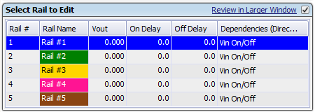 Figure 2. Rail Selection Window (Configure ►Vout Config tab).
Voltage monitoring parameters of the selected rail can be configured under the same Vout Config tab. The configuration window is shown in Figure 3.
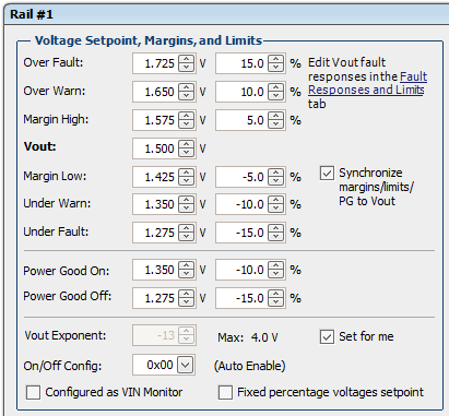 Figure 3. Rail Voltage Configuration Window (Configure ►Vout Config tab).
If a MON pin is assigned in Figure 1 to monitor a rail’s voltage, a warning/fault event will occur when the monitored rail voltage exceeds the voltage window defined by the Over and Under Warn/Fault thresholds. When a fault is detected, UCD90240 will respond with user-defined actions. More details will be discussed in the FAULT RESPONSES CONFIGURATION section.
Vout Exponent defines the voltage value resolution according to PMBus linear data format. Fusion GUI can automatically select optimal Vout Exponent value to cover the required voltage range with the finest possible resolution. For more information regarding PMBus linear data format, refer to PMBus specification mentioned at the beginning of this section.
On/Off Config defines the turnon and turnoff command of a rail:
- None (Auto enable). Rail always seeks to turn on.
- CONTROL Pin Only. Rail seeks to turn on and turn off according to PMBus CONTROL line.
- OPERATION Only. Rail seeks to turn on and turn off according to PMBus OPERATION command.
- Both CONTROL pin and OPERATION. Rail seeks to turn on when CONTROL pin is asserted, AND PMBus OPERATION command sets the rail to On. Rail seeks to turn off when OPERATION command sets the rail to Off, OR when CONTROL line is deasserted, or both.
After a turn on or turn off command is received, a rail examines a series of conditions before asserting or deasserting its EN pin. Conditions include Rail Sequence On/Off Dependency, GPI Sequence On/Off Dependency, Turn-On/Off Delay, and so on. They will be discussed in the RAIL SEQUENCE CONFIGURATION section.
Fixed percentage voltages setpoint, when checked, configures a rail into AVS mode (Adaptive Voltage Scaling Technology). The VOUT setpoint may be dynamically set by PMBus during operation in order to achieve energy saving. The warn and fault voltage thresholds of the rail will maintain fixed ratios with respect to the VOUT setpoint. Due to the fact that the power supply and UCD90240 may not change Vout setpoint simultaneously or with the same slew rate, UCD90240 will take the following steps to avoid false-triggering warn/fault. If the new VOUT setpoint is higher than the current VOUT setpoint, the OV warn/fault thresholds will be immediately set to their respective new levels; other thresholds will initially stay unchanged, and then increase by 20-mV step size every 400 µs until the new levels are reached. If the new VOUT setpoint is lower than the current VOUT setpoint, the UV warn/fault and Power Good On/Off thresholds will be immediately set to their respective new levels; other thresholds will initially stay unchanged, and then decrease by 20-mV step size every 400 µs until the new levels are reached. The thresholds adjustment scheme in AVS mode is summarized in Table 1.
Table 1. Thresholds Adjustment Scheme in AVS Mode
| Immediate Update | Gradual adjustment towards new levels with 20mV step size and 400µs step interval | |
| New VOUT setpoint > Current VOUT setpoint | OV Fault/Warn | UV Fault/Warn, Margin High/Low, Power Good On/Off |
| New VOUT setpoint < Current VOUT setpoint | UV Fault/Warn, Power Good On/Off | OV Fault/Warn, Margin High/Low |
Current and temperature monitoring parameters of the selected rail can be configured under the Fault Responses and Limits tab. First select a rail in the top-right corner of the FUSION GUI, and then edit the current and temperature monitoring parameters as shown in Figure 4.
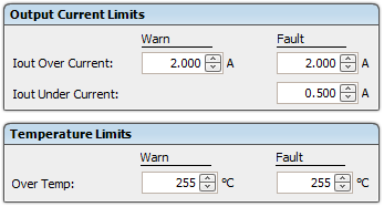 Figure 4. Current and Temperature Limits Configuration Window
 (Configure ► Fault Responses and Limits tab)
Each rail has a Power Good status which is determined by the following rules:
- If rail voltage is monitored by a MON pin, the Power Good status is solely determined by Power Good On/Off thresholds as shown in Figure 3. A rail is given Power Good status if its rail voltage is above the Power Good On threshold. Otherwise, the rail is given Not Power Good status if the rail voltage is below the Power Good Off threshold. The rail remains in the current status if its voltage is neither above Power Good On nor below Power Good Off thresholds.
- If rail voltage is not monitored by a MON pin, the Power Good status is determined by the turnon and turnoff eligibility of the rail. A rail is immediately given Power Good status when the rail meets all the turnon conditions set by the user, such as On/Off Config, dependencies and delays. Similarly, a rail is immediately given Not Power Good status when the rail meets all the turnoff conditions set by the user. The behavior is the same regardless whether a physical EN pin is assigned to the rail.
The Power Good status is not affected by any warnings and faults unless the fault response is to turn off the rail. UV fault/warn is ignored when a rail is off. UV fault/warn is also ignored during start up until the rail enters Power Good status for the first time. This mechanism avoids false-triggering UV fault/warn when the rail voltage is expected to be below UV thresholds.
A Graceful Shutdown feature is enabled by checking the Configured as VIN Monitor checkbox. When enabled, the rail is configured to monitor VIN. When VIN drops below Power Good Off threshold, all other rails’ UV faults/warns will be ignored.
7.3.5 GPI Configuration
UCD90240 has 24 GPIO pins. All of them can be configured as GPI. The GPI configuration window is under the Pin Assignment tab. An example is shown in Figure 5.
 Figure 5. GPI Configuration Window (Configure ►Pin Assignment tab).
The polarity of GPI pins can be configured to be Active High or Active Low. Each GPI can be used as a source of sequence dependency, which will be discussed in the RAIL SEQUENCE CONFIGURATION section. The GPI pins can be also used for cascading function, which will be discussed in CASCADING MULTIPLE DEVICES section. The first defined three GPIs regardless of their main purpose will be used for the Pin Selected States function, which will be discussed in PIN SELECTED STATES section.
In addition to above functions, four special behaviors can be assigned to each GPI pin in the dropdown window shown in Figure 6:
- GPI Fault – The deassertion of this pin is treated as a fault, which can trigger shut-down actions for any voltage rails. More details are discussed in the Fault Responses Configuration section.
- Latched Statuses Clear Source – this pin can be used to clear latched-type statuses (_LATCH). More details are discussed in GPO Configurationsection.
- Input Source for Margin Enable – When this pin is asserted, all rails with margining enabled will be put in a margined state (low or high). No more than one GPI can have this special behavior.
- Input Source for Margin Low/Not-High – When this pin is asserted, all margined rails will be set to Margin Low as long as the Margin Enable is asserted. When this pin is deasserted the rails will be set to Margin High as long as the Margin Enable is asserted. No more than one GPI can have this special behavior.
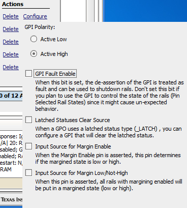 Figure 6. GPI Configuration Dropdown Window (Configure ►Pin Assignment tab).
7.3.6 Rail Sequence Configuration
Rail sequences can be configured in the Vout Config tab. First select a rail in the top-right corner of the FUSION GUI, and then edit the rail sequence as shown in Figure 7.
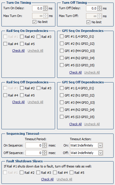 Figure 7. Rail Sequence Configuration Window (Configure ►Vout Config tab).
When a rail receives a turnon or turnoff command as defined in On/Off Config, it will check its dependency conditions. When all dependencies are fulfilled, the rail will then wait for a Turn On/Off Delay time, and then assert/deassert the EN pin.
A Rail Sequence On Dependency is fulfilled when the rail is in Power Good status. A Rail Sequence Off Dependency is fulfilled when the rail is in Not Power Good status. A GPI Sequence On dependency is fulfilled when the GPI pin is asserted. A GPI Sequence Off dependency is fulfilled when the GPI pin is deasserted.
After the EN pin of a rail is asserted, if the rail voltage does not rise above Power Good On threshold within Max Turn On time, a Time On Max fault will occur. Similarly, after the EN pin of a rail is deasserted, if the rail voltage does not fall below 12.5% nominal Vout within Max Turn Off time, a Time Off Max warn will occur.
Each rail can have Fault Shutdown Slaves. When a rail is shut down as a result of a fault, its slave rails will also shut down. The delays and dependencies of the slave rails will still be observed during the shutdown process. Fault Shutdown Slaves cannot cascade. In other words, if a rail is shut down as a slave, it will not shut down its own slave rails.
Each rail can set Sequencing On/Off Timeout periods. The timeout periods start to count when a rail receives a turnon or turnoff command as defined in On/Off Config. When the Sequencing On/Off Timeout period elapsed, the rail will execute one of three actions including:
- Wait Indefinitely
- Enable/Disable Rail
- Re-sequence (Sequencing On only)
Re-sequence is a series of actions that shut down a rail and its Fault Shutdown Slaves, and then re-enable the rails according to sequence-on delay times and dependencies. The Re-sequencing parameters can be configured in the Other Config tab, as shown in Figure 8.
 Figure 8. Re-Sequencing Options (Configure ►Other Config tab).
Re-sequencing can be repeated for 1~4 times or unlimited times. The Time Between Re-Sequences period will start to count when all the relevant rails are given Not Power Good statuses. When the time period elapses, a Re-sequence will start. The Enable Re-Sequence Abort checkbox, when checked, will abort Re-sequence if any relevant rail triggers a Max Turn Off warning. However, the Max Turn Off warning will not stop an ongoing Re-sequence.
When Rail Sequence configurations are completed, simulated sequence timing will be shown in the Vout Config tab. It demonstrates the dependencies among the rails. An example is shown in Figure 9. The power-on/off slew rates of the rail in Figure 9 are for demonstration purpose only.
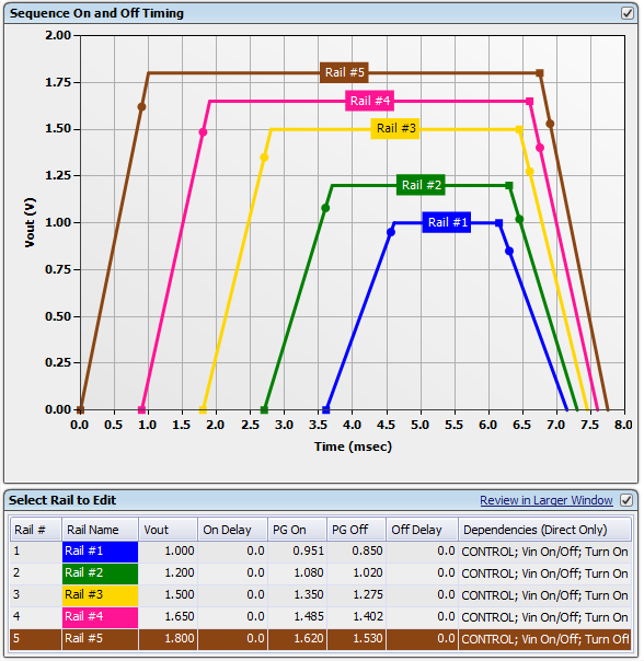 Figure 9. Simulated Sequence Timing Window (Configure ►Vout Config Config tab)
7.3.7 Fault Responses Configuration
In the previous sections, various fault/warning thresholds have been configured to monitor voltage, current, temperature, and turnon and turnoff time. When a fault threshold is reached, a fault event will occur. UCD90240 does three actions in response of a fault event: (1) Assert PMBus ALERT# line, (2) Log the fault event into nonvolatile memory (data flash), (3) Execute fault responses defined by users. The Fault Responses can be configured under the Fault Responses and Limits tab. An example configuration window is shown in Figure 10.
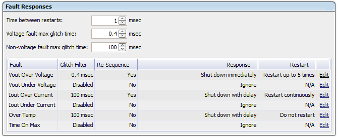 Figure 10. Fault Responses Configuration Window
 (Configure ► Fault Responses and Limits tab).
A programmable glitch filter can be enabled or disabled for each type of fault. If a fault is still present after the glitch filter time is expired, UCD90240 will take one of the three selectable actions:
- Log the fault and take no further action;
- Shut down the rail immediately;
- Shut down the rail with Turn Off Delay.
After shutting down the rail, UCD90240 will do one of the three selectable actions:
- Do not restart the rail until the fault is cleared;
- Restart the rail; if unsuccessful, retry up to a user-defined times (maximum 14) and then stay off until the fault is cleared;
- Restart the rail; if unsuccessful, retry for an unlimited number of times unless the rail is commanded off by a signal defined in On/Off Config.
After the rail exhausts the restart attempts, Re-sequence can be initiated. Discussion on Re-sequence is in the RAIL SEQUENCE CONFIGURATION section.
Voltage, current, and temperature monitoring are based on results from the 12-bit ADC. All the voltage monitoring ADC channels are monitored every 400 µs for up to 24 channels. Current monitoring ADC channels are monitored at 200 µs per channel. Temperature monitoring ADC channels are monitored at ~4.17ms per channel. The ADC results are compared with the programmed thresholds. The time to respond to an individual event is determined by when the event occurs within the ADC conversion cycle and the configured fault responses (glitch filters, time delays, etc.).
GPI pins can also trigger faults if the GPI Fault Enable checkbox in Figure 6 is checked. The GPI Fault Responses options are the same as the Fault Responses discussed above. An example configuration window is shown in Figure 11.
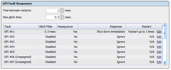 Figure 11. GPI Fault Responses Configuration Window (Configure ► Fault Responses and Limits tab).
7.3.8 GPO Configuration
7.3.8.1 Command Controlled GPO
UCD90240 has 24 GPIO pins, all of which can be configured as Command Controlled GPOs. These GPOs are controlled by PMBus commands (GPIO_SELECT and GPIO_CONFIG) and can be used to control LEDs, enable switches, etc. Details on controlling a GPO using PMBus commands can be found in the UCD90xxx Sequencer and System Health Controller PMBUS Command Reference (SLVU352). The configuration window of Command Controlled GPO is under Pin Assignment tab. An example configuration window is shown in Figure 12.
 Figure 12. Command Controlled GPO Configuration Window (Configure ► Pin Assignments tab).
7.3.8.2 Logic GPO
UCD90240 also has 12 dedicated Logic GPO (LGPO) pins. The configuration window is under Pin Assignment tab, as shown in Figure 13.
 Figure 13. Logic GPO Configuration Window (Configure ► Pin Assignments tab).
Each LGPO is controlled by an internal Boolean logic builder. The configuration interface of the Boolean logic builder is shown in Figure 14. As shown, each Boolean logic builder has a top-level logic gate, which can be configured as AND, OR, or NOR gate with optional time delay. The inputs of the top-level logic gate are two AND paths. Each AND path can select a variety of inputs including GPI states, LGPO states, and rail statuses, as shown in Figure 15. The selectable rail statuses are summarized in Table 2. In Table 2, _LATCH type statuses stay asserted until cleared by a MFR PMBus command or by a specially configured GPI pin shown in Figure 6. See the UCD90xxx Sequencer and System Health Controller PMBUS Command Reference (SLVU352) for complete definitions of rail-status types.
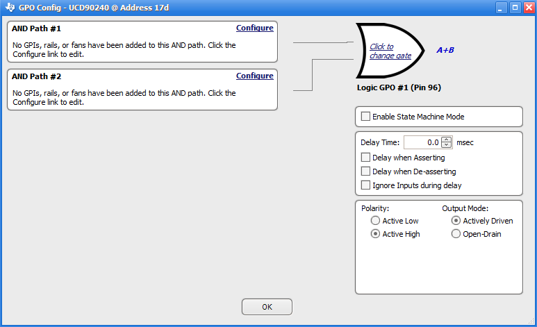 Figure 14. Boolean Logic Builder Interface.
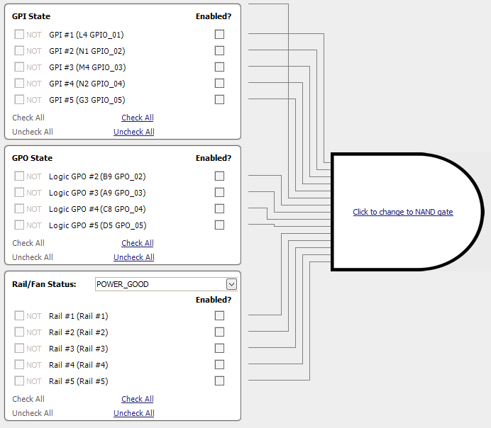 Figure 15. AND Path Configuration.
Table 2. Selectable Rail Statuses in Boolean Logic Builder
| RAIL-STATUS TYPES | ||
|---|---|---|
| POWER_GOOD | IOUT_OC_FAULT | TON_MAX_FAULT |
| MARGIN_EN | IOUT_OC_WARN | TOFF_MAX_WARN |
| MRG_LOW_nHIGH | IOUT_UC_FAULT | TON_MAX_FAULT_LATCH |
| VOUT_OV_FAULT | IOUT_OC_FAULT_LATCH | TOFF_MAX_WARN_LATCH |
| VOUT_OV_WARN | IOUT_OC_WARN_LATCH | SEQ_ON_TIMEOUT |
| VOUT_UV_WARN | IOUT_UC_FAULT_LATCH | SEQ_OFF_TIMEOUT |
| VOUT_UV_FAULT | TEMP_OT_FAULT | SEQ_ON_TIMEOUT_LATCH |
| VOUT_OV_FAULT_LATCH | TEMP_OT_WARN | SEQ_OFF_TIMEOUT_LATCH |
| VOUT_OV_WARN_LATCH | TEMP_OT_FAULT_LATCH | SYSTEM_WATCHDOG_TIMEOUT |
| VOUT_UV_WARN_LATCH | TEMP_OT_WARN_LATCH | SYSTEM_WATCHDOG_TIMEOUT_LATCH |
| VOUT_UV_FAULT_LATCH | ||
Each LGPO can be also configured as a simple state machine. The configuration checkbox is in shown in Figure 14. In state machine mode, the top-level logic gate is omitted; only one of the two AND paths will be evaluated; the output of the state machine is the result of the active AND Path. The evaluation initially starts with AND Path #1. If the evaluation result is TRUE, AND Path #1 will stay active until its evaluation result becomes FALSE. When AND Path#1’s output becomes FALSE, AND Path #2 will be become active in the next evaluation cycle. AND Path #2 will stay active until its evaluation result becomes TRUE, then AND Path #1 will become active in the next evaluation cycle. An evaluation cycle is triggered when any input signal to the state machine changes state.
GPO1 to GPO8 outputs are internally synchronized to the same clock edge to change states together. GPO9 to GPO12 outputs are internally synchronized and change states together. GPO 1-8 and GPO 9-12 outputs status are updated within a 1~3 µs window.
7.3.9 Margining Configuration
UCD90240 can provide accurate closed-loop margining for up to 24 voltage rails. System reliability can be improved through four-corner testing during system verification. During four-corner testing, the system is operated at the minimum and maximum expected ambient temperature and with each power supply set to the minimum and maximum output voltage, commonly referred to as margining. Margining can be controlled over PMBus using the OPERATION command or by configuring two GPI pins as margin-EN and margin-UP/DOWN inputs. The MARGIN_CONFIG command in the UCD90xxx Sequencer and System Health Controller PMBus Command Reference describes several margining options, including ignoring faults while margining and using closed-loop margining to trim the rail output voltage.
UCD90240 provides 24 PWM output pins for closed-loop margining. A block diagram of margining circuit is shown in Figure 16. An external RC network converts the PWM pulses into a DC margining voltage. The margining voltage is connected to the power supply’s feedback node through a resistor. The feedback node voltage is thus slightly pulled up/down by the margining voltage, causing the rail output voltage to change. The rail output voltage is monitored by UCD90240, and the margining PWM duty cycle is adjusted accordingly such that the rail output voltage is regulated at the margin-high/low voltages defined by the user. Effectively, the DC set point of the margined power supply is overwritten by UCD90240’s margin control loop. The margin control loop is extremely slow such that it does not interfere with the power supply’s control loop.
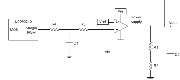 Figure 16. Block Diagram of Margining Circuit
Margining pins can be configured under the Pin Assignment tab, as shown in Figure 17. When not margining, the margin pin can operate in one of three modes: Tri-State, Active Trim, and Active Duty Cycle. Tri-State mode will set the margin pin to high-impedance. Active Trim mode will continuously trim the DC output voltage. Active Duty Cycle mode will provide a user-defined fixed PWM duty cycle as shown in Figure 17.
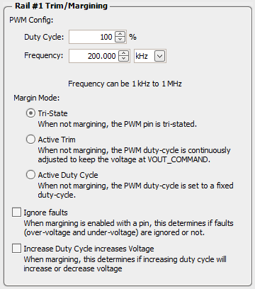 Figure 17. Margining Configuration Dropdown Window
 (Configure ►Pin Assignment tab)
7.3.10 Pin Selected Rail States Configuration
UCD90240 allows users to use up to three GPI pins to control up to eight rail states. Each rail state enables and disables certain rails. This feature is useful to implement system low-power modes, such as those compliant with the Advanced Configuration and Power Interface (ACPI) specification. The Pin Selected States function can be configured under the Pin Selected States tab, as shown in Figure 18.
If a new state is presented on the GPI pins, and a rail is commanded to turn on, it will do so according to its sequence-on dependencies and delays. If a rail is commanded to turn off by a new state, it can be configured to immediately turn off (Immediate Off), or to turn off with its sequence-off dependencies and delays (Soft Off). If a rail is commanded to remain in the same on/off state, no action will take place.
The Pin Selected Rail States function is implemented by modifying OPERATION command. Therefore, in order to use this function to control rail states, the related rails must be configured to use OPERATION command in On/Off Config (shown in Figure 3).
The Pin Selected States feature always uses the first three configured GPI pins to select system states. When selecting a new system state, state changes on GPI pins must be completed within 1 µs, otherwise an unintended system state may be selected. See the UCD90xxx Sequencer and System Health Controller PMBus Command Reference for complete configuration settings of Pin Selected States.
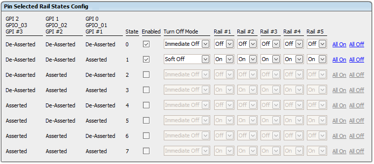 Figure 18. Pin Selected States Configuration Window (Configure ►Pin Assignment tab)
7.3.11 Watchdog Timer
UCD90240 provides a watchdog timer (WDT). The WDT can be reset by toggling a watchdog input (WDI) pin. If WDI is not toggled within a programmed period, the WDT will time out. As a result, a watchdog output (WDO) pin will be asserted (or generate a pulse) in order to provide a system-reset signal.
The WDI and WDO pins are GPIO pins and are only optional. The WDI can be replaced by SYSTEM_WATCHDOG_RESET command sent over PMBus. The WDO can be manifested through the Boolean Logic defined GPOs, or its function can be integrated into the System Reset pin configured in the System Reset function (System Reset function will be discussed in the SYSTEM RESET FUNCTION section).
The WDT timer is programmable from 0.001s to 258.048s. See the UCD90xxx Sequencer and System Health Controller PMBus Command Reference for details on configuring the watchdog timer.
After a timeout, the WDT can be restarted by toggling the WDI pin or by writing a SYSTEM_WATCHDOG_RESET command over PMBus. A watchdog timing diagram is shown in Figure 19.
 Figure 19. Watchdog Timer Operation Timing Diagram
The WDT can be active immediately at power up or has an initial wait time. Table 3 lists the programmable wait times before the WDT operation begins.
Table 3. WDT Initial Wait Time
| 0 ms |
| 100 ms |
| 200 ms |
| 400 ms |
| 800 ms |
| 1.6 s |
| 3.2 s |
| 6.4 s |
| 12.8 s |
| 25.6 s |
| 51.2 s |
| 102.4 s |
| 204.8 s |
| 409.6 s |
| 819.2 s |
| 1638.4 s |
7.3.12 System Reset Function
System Reset function can generate a programmable System Reset signal through a GPIO pin. The System Reset signal is deasserted when the selected rail voltages reach their respective Power Good On thresholds and the selected GPIs are asserted, plus a programmable delay time. Available options for the system-reset delay time are summarized in Table 4.
The System Reset signal can be asserted immediately when any of the selected rail voltage falls below Power Good Off threshold, or any selected GPI is deasserted. Alternatively, the System Reset signal can be configured as a pulse once Power Good On is achieved. An example in Figure 20 illustrates the difference of the two configurations. The pulse width can be configured between 0.001 s to 32.256 s. See the UCD90xxx Sequencer and System Health Controller PMBus Command Reference for pulse width configuration details.
 Figure 20. System Reset with and without Pulse Setting (Active Low).
The System Reset signal can also integrate watchdog timer. An example is shown in Figure 21. In Figure 21, the first delay on System Reset is for the initial reset release that would enable the CPU once all necessary voltage rails are Power Good. The watchdog is configured with a Start Time and a Reset Time. If these times expire and timeout occurs, it means that the CPU providing the WDI signal is not operating. The System Reset signal is then toggled either using a Delay or GPI Tracking Release Delay to see if the CPU recovers.
 Figure 21. System Reset with Watchdog
Table 4. System Reset Delay
| DELAY |
|---|
| 0 ms |
| 1 ms |
| 2 ms |
| 4 ms |
| 8 ms |
| 16 ms |
| 32 ms |
| 64 ms |
| 128 ms |
| 256 ms |
| 512 ms |
| 1.02 s |
| 2.05 s |
| 4.10 s |
| 8.19 s |
| 16.38 s |
| 32.8 s |
The default state of the System Reset pin is Assert. When the System Reset function is configured in-circuit via PMBus commands during normal operation, the System Reset pin will briefly assert by default, even if conditions for deassert are present. This is because the firmware requires a finite time to examine the deassert conditions.
7.3.13 Cascading Multiple Devices
Multiple UCD90240 devices can work together and coordinate when faults happen
Up to four GPI pins can be configured as Fault Pins. Each Fault Pin is connected to a Fault Bus. Each Fault Bus is pulled up to 3.3 V by a 10-kΩ resistor. All the UCD90240 devices on the same Fault Bus are informed of the same fault condition. An example of Fault Pin connections is shown in Figure 22.
When there is no fault on a Fault Bus, the Fault Pins are digital input pins and listen to the Fault Bus. When one or multiple UCD90240 devices detect a rail fault, the corresponding Fault Pin is turned into active driven low state, pulling down the Fault Bus and informing all other UCD90240 devices of the corresponding fault. This way, a coordinated action can be taken across multiple devices. After the fault is cleared, the state of the Fault Pin is turned back to an input pin.
Any of the 24 rails can be assigned to one or multiple Fault Pins. The configuration window is shown in Figure 23.
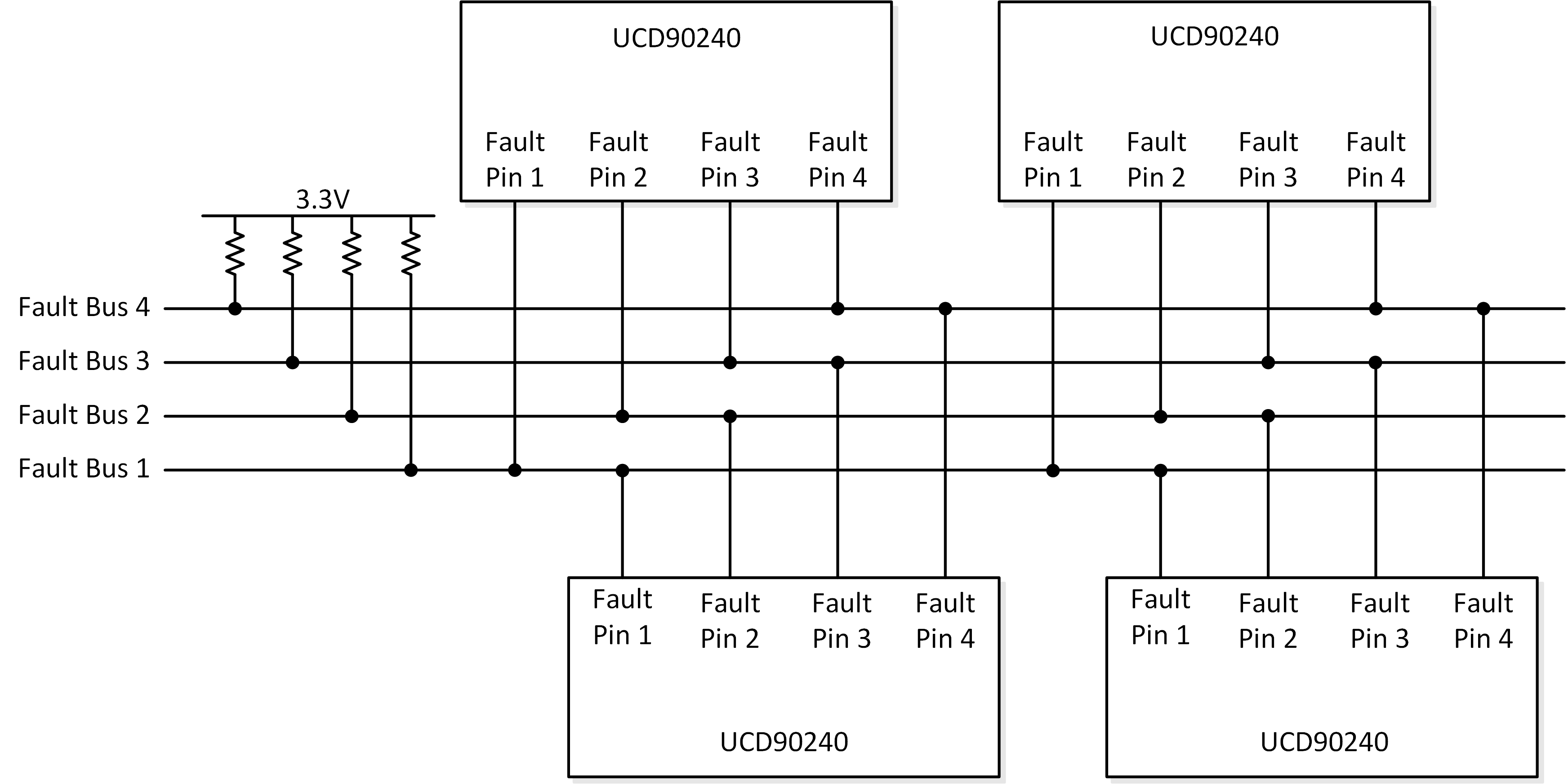 Figure 22. Example of Fault Pin Connections
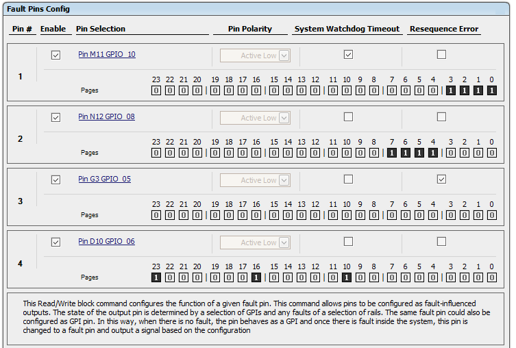 Figure 23. Example Fault Pins Configuration Window (Configure ►Fault Pins tab)
A SYNC_CLK pin is used as a single-wire time synchronization method. A Master chip constantly drives a 5kHz clocks to the Slave devices. This offers a precise time base for multiple UCD90240 devices to respond to the same fault event at the same time. The configuration window is shown in Figure 24. If the system only consists of a single UCD90240, it is recommended to configure this pin as master clock output. The SYNC_CLK output can be used as a time base for other purposes if needed.
 Figure 24. Sync Clock Configuration (Configure ►Other Config tab)
7.3.14 Voltage Monitoring
UCD90240 monitors up to 24 analog inputs including voltages, current, and temperature. FUSION GUI or a PMBus host can poll data from UCD90240. FUSION GUI displays monitored rail voltage, current, and temperature information on its Monitor page. This is especially useful for debugging system-level issues. The Monitor page interface is shown in Figure 25.
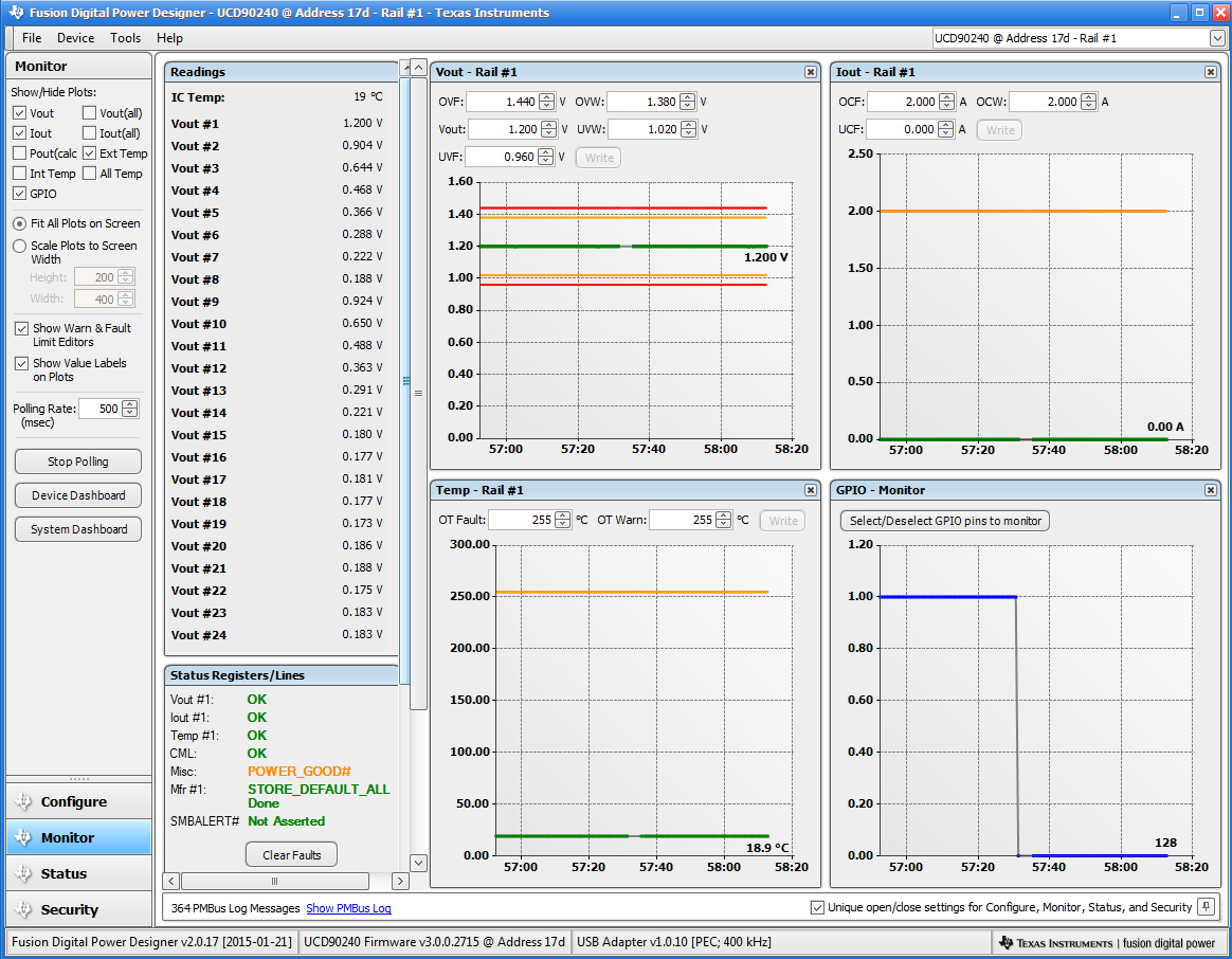 Figure 25. Fusion GUI Monitor Page
7.3.15 Status Monitoring
The UCD90240 has status registers for each rail. Faults and warnings are logged into EEPROM memory to assist system troubleshooting. The status registers (Figure 26) and the fault log (Figure 27) can be accessed from Fusion GUI as well as PMBus. See the UCD90xxx Sequencer and System Health Controller PMBus Command Reference (SLVU352) and the PMBus Specification for detailed descriptions of each status register and supported PMBus commands.
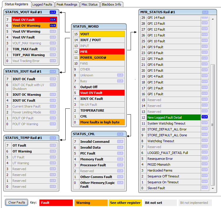 Figure 26. Fusion GUI Rail Status Registers (Status ►Status Registers tab)
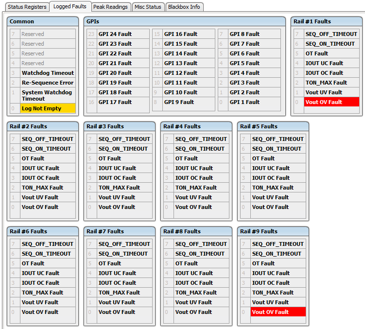 Figure 27. Fusion GUI Logged Faults(Status ►Logged Faults tab)
7.3.16 Data and Error Logging to EEPROM Memory
The UCD90240 provides fault log, device reset counter, and peak readings for each rail. To reduce stress on the EEPROM memory, a 30-second timer is started if a measured value exceeds the previously logged value. Only the highest value from the 30-second interval is written from RAM to EEPROM.
Faults are stored in EEPROM memory and are accessible over PMBus. Each logged fault includes the following information:
- Rail number
- Fault type
- Fault time since previous device reset
- Last measured rail voltage
The total number of device resets is also stored to EEPROM memory. The value can be reset using PMBus.
The runtime clock value is logged into EEPROM when a power down is detected. This allows UCD90240 to preserve the runtime clock value through resets or power cycles.
It is also possible to update and calibrate the UCD90240 internal runtime clock via a PMBus host. For example, a host processor with a real-time clock could periodically update the UCD90240 runtime clock to a value that corresponds to the actual date and time. The host must translate the UCD90240 timer value back into appropriate units, based on the usage scenario chosen. See the REAL_TIME_CLOCK command in the UCD90xxx Sequencer and System Health Controller PMBus Command Reference for more details.
7.3.17 Black Box First Fault Logging
The first fault in a system failure event is usually critical to diagnose the root cause. An innovative Black Box Fault Logging feature is introduced in UCD90240 to accelerate the debugging process. When UCD90240 detects the first fault, all rails’ and I/O pins’ statuses are saved into a special area of EEPROM that is reserved for this function. The subsequent faults and monitoring statuses will not be saved in the Black Box Fault Log, but they will still be logged into the standard fault log. The Black Box Fault Log must be cleared in order to catch the next fault.
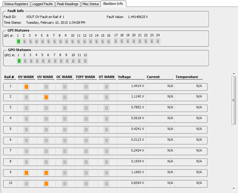 Figure 28. Black Box Fault Logging Window (Status ►Blackbox Info tab)
7.3.18 PMBUS Address Selection
Three digital input pins are allocated to decode the PMBus address. At power up, UCD90240 detects the logic inputs of the three address pins to determine the configured PMBus address.
Table 5. PMBus Address Configuration
| PMBUS_ADDR2 | PMBUS_ADDR1 | PMBUS_ADDR0 | PMBus ADDRESS SELECTED | |
|---|---|---|---|---|
| L | L | L | 17d | 00010001b |
| L | L | H | 19d | 00010011b |
| L | H | L | 23d | 00010111b |
| L | H | H | 49d | 00110001b |
| H | L | L | 51d | 00110011b |
| H | L | H | 113d | 01110001b |
| H | H | L | 115d | 01110011b |
| H | H | H | 119d | 01110111b |
UCD90240 is a PMBus slave but it does not support slave arbitration. Multiple PMBus devices including UCD90240 can work on the same PMBus if all the PMBus addresses meet the following requirement: when perform binary AND operation to any two of the addresses on the bus, the result must always be the lowest address. See UCD90240 application notes for details.
7.3.19 ADC Reference
UCD90240 uses V33A as ADC reference voltage by default. This provides a cost-effective solution. However, internal voltage reference has higher Total Unadjusted Error. Also, voltage variations on V33A will affect ADC readings, such as when the device is powered down. In order to achieve better ADC accuracy, an external voltage reference can be connected to the VREFA+ and VREFA– pins. The external reference voltage should stay in regulation whenever V33D is above VBOR threshold. This allows accurate ADC readings in full V33D operating range.
The external reference voltage level must be configured into the Fusion GUI to give correct ADC readings.
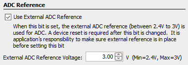 Figure 29. ADC Reference Configuration Window (Configure ►Other Config tab)
7.3.20 Device Reset
The UCD90240 has an integrated power-on reset (POR) circuit which monitors the supply voltage. At power up, the POR detects the V33D rise. When V33D is greater than VRESET, the device comes out of reset.
The device can be forced into the reset state by an external circuit connected to the RESET pin. A logic-low voltage on this pin for longer than tRESET sets the device into reset state. The device comes out of reset within tIRT after RESET is released to logic-high level.
Any time the device comes out of reset, it begins an initialization routine that lasts typically 27.5 ms. A data flash checksum verification is performed at power up. If the checksum does not match, the device configuration will be wiped out, the PMBALERT# pin will be asserted, and a flag will be set in the status register. A fault-log checksum verification in EEPROM is also performed at power up. Each log entry has a checksum. Only the corrupted log entry will be discarded. During the initialization routine, all I/O pins are held at high impedance state. At the end of initialization, the device begins normal operation as defined by the device configuration.
7.3.21 Brownout
UCD90240 triggers brownout event when V33D drops below VBOR. During brownout, the device continues to write fault logs that happened before the brownout event into the EEPROM. As the supply voltage continues to drop, the device will fully shutdown when V33D is below VSHDN. Any fault event that has not been written into the EEPROM before the device shutdown will be lost.
In the scenario where several faults happen immediately before the brownout event, the device requires 500µs to write the first fault event into the EEPROM, and additional 4ms to write the Black Box fault log into the EEPROM. Therefore, in order to preserve at least the first fault log, user must provide enough local capacitance to maintain the V33D rail above VSHDN for 500 µs (or 4.5ms with the Black Box fault log). Longer holdup time allows more fault events to be written into the EEPROM during brownout. Note that the holdup time is affected by V33D rail capacitance, UCD90240’s supply current and external circuits that source current from the rail (for example, LEDs, load current on I/O pins, other devices powered by the same rail, and so forth).
 Figure 30. Reset and Brownout Thresholds
7.3.22 Device Configuration and Programming
UCD90240 devices come out of factory with the sequencing and monitoring firmware. They are also configured in such a way that all I/O pins are high-impedance, with no sequencing or fault-response operation. User can use Fusion GUI to configure the device on-line or off-line. Once the configuration is completed, user can generate a configuration file, and import the configuration into other UCD90240 devices
Configuration and programming details are described in Configuration Programming of UCD Devices which is available in Documentation & Help Center under Fusion GUI’s Help menu. In general, UCD90240 supports two programming methods:
- PMBus command over PMBus/I2C.
- Data flash image over PMBus/I2C.
This method uses a PMBus host to program the device. The PMBus host can be either a host microcontroller or Fusion GUI tools. Each PMBus command sends a corresponding parameter(s) into the device. The new parameters are stored in its associated memory (RAM) location. After all the parameters are sent into the device, the PMBus host issues a special command, STORE_DEFAULT_ALL, which writes the RAM data into nonvolatile memory (data flash). Fusion GUI normally uses this method to configure a device. Note that, if use Fusion GUI tools for on-board programming, the Fusion GUI tools must have ownership of the target board’s PMBus/I2C bus.
The Fusion GUI can export a data flash image in Intel Hex or S-record format. The image file can be directly downloaded into the device’s data flash via PMBus/I2C using Fusion GUI tools or a dedicated device programmer. The new configuration will take effect after a device reset.
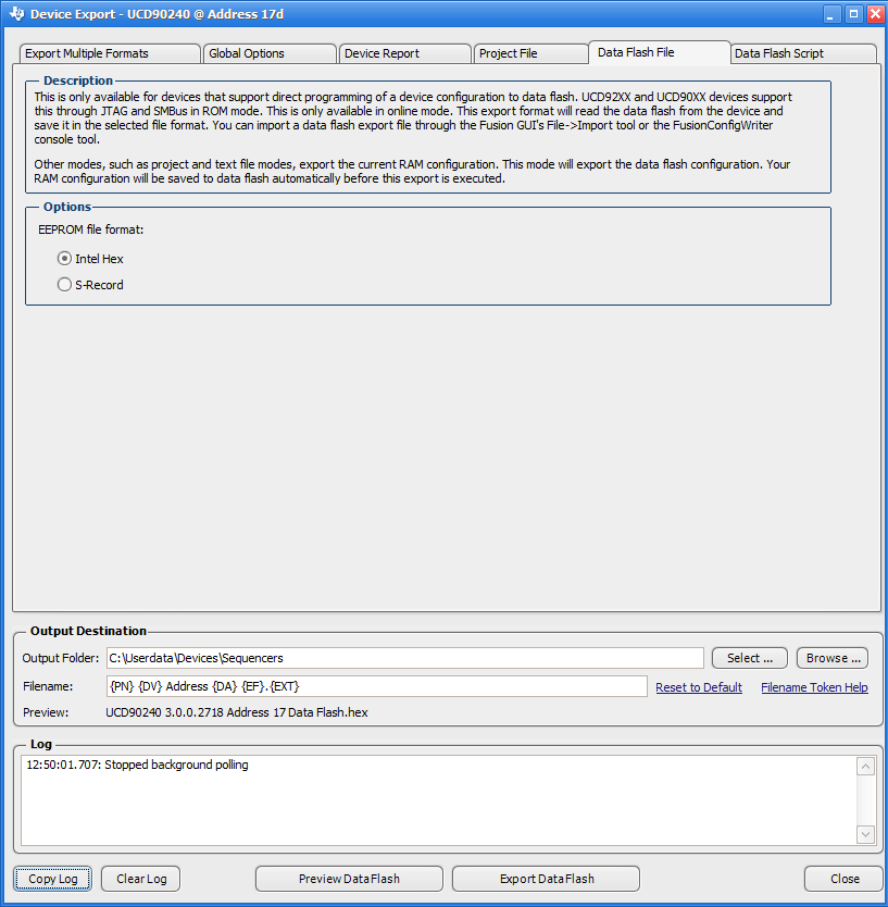 Figure 31. Fusion GUI Configuration Export Tool.
While programming over PMBus /I2C, the UCD90240 must be powered. The PMBus clock and data pins must be accessible and must be pulled high to the same V33D supply that powers the device, with pullup resistors between 1 kΩ and 2 kΩ. Care should be taken to not introduce additional bus capacitance (<100 pF). When use gang programmer to program multiple UCD90240 devices over I2C, programming must be done individually: the clock and data lines must be multiplexed such that only one device is written by the programmer at a time; alternatively, the socket must assign different addresses to each device. For small runs, a socketed board with an I2C header can be used with the standard Fusion GUI or manufacturing GUI. Programming also can be done using a single device test fixture.
There may be situations where it is required to update the device configuration in an operating system. The PMBus command method can be used to update thresholds, timeout periods, dependencies, and so forth, while the system is operating. Because the new configuration is written into RAM, it will take effect immediately. However, pin-function-related configurations (for example, change of rails, change of GPI/GPO functions, and so forth) may not work correctly until a device reset. This may be a problem in an operating system. For example, undesired GPI/GPO/System Reset pin states may disable rails that provide power to the UCD90240, and thus terminate the programming process before it is completed. The data flash image method can overcome this problem by directly writing new configuration into the data flash. This allows a full configuration while the system is operating. It is not required to reset the device immediately but the UCD90240 will continue to operate based on previous configuration until a device reset.
The JTAG port is compatible with IEEE Standard 1149.1-1990, Test-Access Port and Boundary Scan Architecture specification. UCD90240 supports boundary scan. Configuration programming via JTAG is not supported on this device.
7.3.23 Internal Fault Management
The UCD90240 verifies the firmware program checksum at each power up. If the checksum does not match, the device will reset. If the device keeps resetting, the SYNC_CLK pin will output repeated pulses with ~250-ms pulse width that can be observed externally.
The configuration data checksum verification is also performed at power up. If the checksum does not match, the device will wipe out all the configuration data. The PMBALERT# pin is asserted and a flag is set in the status register.
A fault-log checksum verification in EEPROM is also performed at power up. Each log entry has a checksum. The corrupted log entry will be discarded.
There is an internal firmware watchdog timer. If it times out, the device resets so that if the firmware program is corrupted, the device goes back to a known state. This is a normal device reset, so all of the I/O pins are held in high-impedance while the device is in reset. Checks are also done on each parameter that is passed, to make sure it falls within the acceptable range.