ZHCSDF1 February 2015 UCD90240
PRODUCTION DATA.
- 1 特性
- 2 应用
- 3 说明
- 4 修订历史记录
- 5 Pin Configuration and Functions
- 6 Specifications
-
7 Detailed Description
- 7.1 Device Overview
- 7.2 Functional Block Diagram
- 7.3
Feature Description
- 7.3.1 TI Fusion GUI
- 7.3.2 PMBUS Interface
- 7.3.3 Rail Setup
- 7.3.4 Rail Monitoring Configuration
- 7.3.5 GPI Configuration
- 7.3.6 Rail Sequence Configuration
- 7.3.7 Fault Responses Configuration
- 7.3.8 GPO Configuration
- 7.3.9 Margining Configuration
- 7.3.10 Pin Selected Rail States Configuration
- 7.3.11 Watchdog Timer
- 7.3.12 System Reset Function
- 7.3.13 Cascading Multiple Devices
- 7.3.14 Voltage Monitoring
- 7.3.15 Status Monitoring
- 7.3.16 Data and Error Logging to EEPROM Memory
- 7.3.17 Black Box First Fault Logging
- 7.3.18 PMBUS Address Selection
- 7.3.19 ADC Reference
- 7.3.20 Device Reset
- 7.3.21 Brownout
- 7.3.22 Device Configuration and Programming
- 7.3.23 Internal Fault Management
- 8 Application and Implementation
- 9 Power Supply Recommendations
- 10Layout
- 11器件和文档支持
- 12机械封装和可订购信息
8 Application and Implementation
NOTE
Information in the following applications sections is not part of the TI component specification, and TI does not warrant its accuracy or completeness. TI’s customers are responsible for determining suitability of components for their purposes. Customers should validate and test their design implementation to confirm system functionality.
8.1 Application Information
The UCD90240 can be used to sequence, monitor and margin up to 24 voltage rails. With the cascading feature, up to four UCD90240 devices can manage up to 96 rails and take synchronized fault responses. Typical applications include automatic test equipment, telecommunication and networking equipment, servers and storage systems, and so forth. Device configuration can be performed in Fusion GUI. No coding skill is required.
8.2 Typical Application
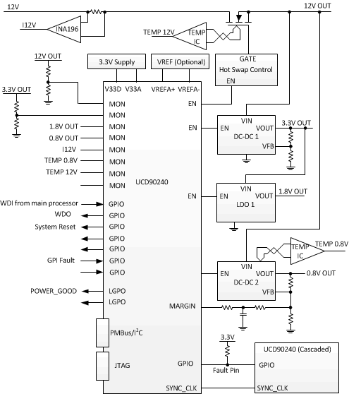
Figure 32 shows a simplified system diagram. Only three rails are shown for illustration purpose. Each UCD90240 device can manage up to 24 rails.
8.2.1 Application Diagram
 Figure 32. Simplified System Diagram
8.2.2 Design Requirements
- UCD90240 requires decoupling capacitors on V33D, V33A, BPCAP, and (if applicable) VREFA+ pins. The capacitance values for V33A, BPCAP and VREFA+ are specified in the Electrical Characteristics section. The following design can be used as a reference:
- Three 1-μF X7R ceramic capacitors in parallel with two 0.1-μF X7R ceramic capacitors for BPCAP decoupling
- Two 1-μF X7R ceramic capacitors in parallel with four 0.1-μF X7R ceramic capacitors and two 0.01-μF X7R ceramic capacitors for V33D decoupling
- One 1-μF X7R ceramic capacitor in parallel with one 0.1-μF X7R ceramic capacitor and one 0.01-μF X7R ceramic capacitor for V33A decoupling. A 1-Ω resistor can placed between V33D and V33A to decouple the noise on V33D from V33A.
- One 1-μF X7R ceramic capacitor in parallel with one 0.01-μF X7R ceramic capacitor for VREFA+ decoupling (if used)
Decoupling capacitors should be placed as close to the device as possible.
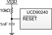
- If an application does not use the RESET signal, the RESET pin must be tied to V33D, either by direct connection to the nearest V33D pin (Pin F10), or by a RC circuit as shown in Figure 33. The RC circuit in Figure 33 can be also used to delay reset at power up.
- It is recommended to maintain at least 200-Ω resistance between a low-impedance analog input and a MON pin. For example, when monitoring a rail voltage without resistor divider, it is recommended to place a 200-Ω resistor at the MON pin, as shown in Figure 34.
If an application uses the RESETexternal pin, the trace of the RESET signal must be kept as short as possible. Be sure to place any components connected to the RESET signal as close to the UCD90240 as possible.
 Figure 33. Example of RESET with RC Circuit
 Figure 34. Example of Analog Inputs
8.2.3 Detailed Design Procedure
Fusion GUI can be used to design the device configuration online or offline (with or without a UCD90240 device connected to the computer). In offline mode, Fusion GUI will prompt user to create or open a project file (.xml) at launch. In online mode, Fusion GUI will automatically detect the device on PMBus and extract the configuration data from the device. An USB Interface Adapter EVM (HPA172) from TI is required to connect Fusion GUI to PMBus.
The general design steps include (1) Rail setup, (2) Rail monitoring configuration, (3) GPI configuration, (4) Rail sequence configuration, (5) Fault response configuration, (6) GPO configuration, (7) Margining configuration, (8) Other configurations such as Pin Selected Rail States, Watchdog Timer, System Reset, Sync Clock, Fault Pins, and so on. Details of the steps are described in the Feature Description section, and are self-explanatory in Fusion GUI.
After configuration change(s), the user should click the Write to Hardware button to apply the changes. In online mode, the user can then click the Store RAM to Flash button to permanently store the new configuration into the data flash of the device.