ZHCSFI3B August 2016 – May 2019 UCD90320
PRODUCTION DATA.
- 1 特性
- 2 应用
- 3 说明
- 4 修订历史记录
- 5 说明 (续)
- 6 Pin Configuration and Functions
- 7 Specifications
-
8 Detailed Description
- 8.1 Overview
- 8.2 Functional Block Diagram
- 8.3 Feature Description
- 8.4
Device Functional Modes
- 8.4.1 Rail Monitoring Configuration
- 8.4.2 GPI Configuration
- 8.4.3 Rail Sequence Configuration
- 8.4.4 Fault Responses Configuration
- 8.4.5 GPO Configuration
- 8.4.6 Margining Configuration
- 8.4.7 Pin Selected Rail States Configuration
- 8.4.8 Watchdog Timer
- 8.4.9 System Reset Function
- 8.4.10 Cascading Multiple Devices
- 8.4.11 Rail Monitoring
- 8.4.12 Status Monitoring
- 8.4.13 Data and Error Logging to EEPROM Memory
- 8.4.14 Black Box First Fault Logging
- 8.4.15 PMBus Address Selection
- 8.4.16 ADC Reference
- 8.4.17 Device Reset
- 8.4.18 Brownout
- 8.4.19 Internal Fault Management
- 8.5 Device Configuration and Programming
- 9 Application and Implementation
- 10Power Supply Recommendations
- 11Layout
- 12器件和文档支持
- 13机械、封装和可订购信息
8.5 Device Configuration and Programming
UCD90320 devices include factory-installed sequencing and monitoring firmware. All I/O pins are pre-configured ad high-impedance, with no sequencing or fault-response operation. Use the Fusion Digital Power Designer software to configure the device on-line or off-line. Generate a configuration file after configuring the device and import that configuration into other UCD90320 devices.
The Configuration Programming of UCD Devices section of the Documentation & Help Center offers configuration and programming details and can be accessed under the Fusion Digital Power Designer software Help menu. In general, UCD90320 supports two programming methods:
- The PMBus command over PMBus and I2C method uses a PMBus host to program the device. The PMBus host can be either a host microcontroller or Fusion Digital Power Designer software tools. Each PMBus command sends a corresponding parameter(s) into the device. The new parameters are stored in its associated memory (RAM) location. After all the parameters are sent into the device, the PMBus host issues a special command, STORE_DEFAULT_ALL, which writes the RAM data into nonvolatile memory (data flash). Fusion GUI normally uses this method to configure a device. If using Fusion Digital Power Designer software tools for on-board programming, the Fusion Digital Power Designer software tools must have ownership of the PMBus/I2C bus of the target board. This method may cause unexpected behaviors on GPIO pins which can disable rails that provide power to device. It is not recommended for production programming.
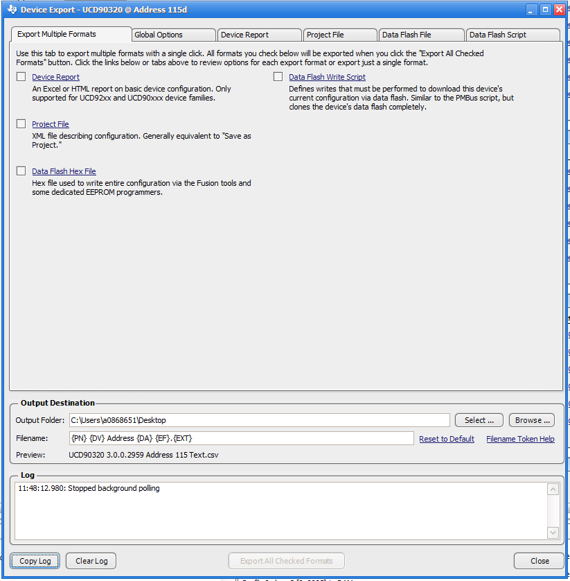
- The data flash image over PMBus and I2C method uses the Fusion Digital Power Designer software to export a data flash image in Intel Hex, CSV or S-record format. The image file can be directly downloaded into the device’s data flash via PMBus and I2C using Fusion Digital Power Designer software tools or a dedicated device programmer. The new configuration takes effect after a device reset. It is recommended to use for production programming since GPIO pins are under controlled state.
 Figure 37. Fusion Digital Power Designer software Configuration Export Tool
 The UCD90320 must be powered when it is being programmed via the PMBus or I2C interface. The PMBus clock and data pins must be accessible and must be pulled high to the same V33D supply that powers the device, with pullup resistors between 1 kΩ and 2 kΩ. Do not introduce additional bus capacitance less than 100 pF. When programming multiple UCD90320 devices over I2C, programming must be done individually. Specifically, the clock and data lines must be multiplexed such that only one device is written by the programmer at a time.
To update the device configuration in an operating system, the PMBus command method can be used to update thresholds, timeout periods, and dependencies while the system is operating. Because the new configuration is written into RAM, it takes effect immediately. However, pin-function-related configurations (change of rails, change of GPI/GPO functions for example) may not work correctly until after a device reset. This delay may indicate a problem in an operating system. For example, undesired states in the GPI, GPO, or RESET pin may disable rails that provide power to the UCD90320, and thus terminate the programming process before it is completed. Using the data flash image method can overcomes this problem by directly writing new configuration into the data flash. This method allows a full configuration while the system is operating. It is not required to reset the device immediately but the UCD90320 continues to operate based on previous configuration until a device reset.
The JTAG port is compatible with IEEE Standard 1149.1-1990, Test-Access Port and Boundary Scan Architecture specification. The UCD90320 device supports boundary scan. The UCD90320 device supports does not support configuration programming via JTAG.