ZHCSFJ6B August 2016 – March 2022 UCD9090A
PRODUCTION DATA
- 1 特性
- 2 应用
- 3 说明
- 4 Revision History
- 5 Pin Configuration and Functions
- 6 Specifications
-
7 Detailed Description
- 7.1 Overview
- 7.2 Functional Block Diagram
- 7.3 Feature Description
- 7.4
Device Functional Modes
- 7.4.1 Power Supply Sequencing
- 7.4.2 Pin-Selected Rail States
- 7.4.3 Monitoring
- 7.4.4 Fault Responses and Alert Processing
- 7.4.5 Shut Down All Rails and Sequence On (Resequence)
- 7.4.6 GPIOs
- 7.4.7 GPO Control
- 7.4.8 GPO Dependencies
- 7.4.9 GPI Special Functions
- 7.4.10 Power Supply Enables
- 7.4.11 Cascading Multiple Devices
- 7.4.12 PWM Outputs
- 7.4.13 Programmable Multiphase PWMs
- 7.4.14 Margining
- 7.4.15 Run Time Clock
- 7.4.16 System Reset Signal
- 7.4.17 Watch Dog Timer
- 7.4.18 Data and Error Logging to Flash Memory
- 7.4.19 Brownout Function
- 7.4.20 PMBus Address Selection
- 7.4.21 Device Reset
- 7.4.22 JTAG Interface
- 7.4.23 Internal Fault Management and Memory Error Correction (ECC)
- 7.5 Programming
- 8 Application and Implementation
- 9 Power Supply Recommendations
- 10Layout
- 11Device and Documentation Support
- 12Mechanical, Packaging, and Orderable Information
封装选项
请参考 PDF 数据表获取器件具体的封装图。
机械数据 (封装 | 引脚)
- RGZ|48
散热焊盘机械数据 (封装 | 引脚)
- RGZ|48
订购信息
7.4.4 Fault Responses and Alert Processing
The UCD9090A monitors whether the rail stays within a window of normal operation.. There are two programmable warning levels (under and over) and two programmable fault levels (under and over). When any monitored voltage goes outside of the warning or fault window, the PMBALERT# pin is asserted immediately, and the appropriate bits are set in the PMBus status registers (see Figure 7-4). Detailed descriptions of the status registers are provided in the UCD90xxx Sequencer and System Health Controller PMBus Command Reference and the PMBus Specification.
A programmable glitch filter can be enabled or disabled for each MON input. A glitch filter for an input defined as a voltage can be set between 0 and 102 ms with 400-μs resolution. The glitch filter only applies to fault responses; a fault condition that is filtered by the glitch filter will still be recorded in the fault log.
Fault-response decisions are based on results from the 12-bit ADC. The device cycles through the ADC results and compares them against the programmed limits. The time to respond to an individual event is determined by when the event occurs within the ADC conversion cycle and the selected fault response.
 Figure 7-11 Sequencing and Fault-Response Timing
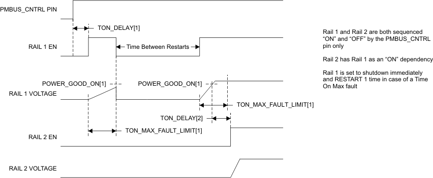
 Figure 7-12 Maximum Turn-On Fault
The configurable fault limits are:
TON_MAX_FAULT – Flagged if a rail that is enabled does not reach the POWER_GOOD_ON limit within the configured time
VOUT_UV_WARN – Flagged if a voltage rail drops below the specified UV warning limit after reaching the POWER_GOOD_ON setting
VOUT_UV_FAULT – Flagged if a rail drops below the specified UV fault limit after reaching the POWER_GOOD_ON setting
VOUT_OV_WARN – Flagged if a rail exceeds the specified OV warning limit at any time during startup or operation
VOUT_OV_FAULT – Flagged if a rail exceeds the specified OV fault limit at any time during startup or operation
MAX_TOFF_WARN – Flagged if a rail that is commanded to shut down does not reach 12.5% of the nominal rail voltage within the configured time
Faults are more serious than warnings. The PMBALERT# pin is always asserted immediately if a warning or fault occurs. If a warning occurs, the following takes place:
| Warning Actions | ||
| — | Immediately assert the PMBALERT# pin | |
| — | Status bit is flagged | |
| — | Assert a GPIO pin (optional) | |
| — | Warnings are not logged to flash | |
| A number of fault response options can be chosen from: | ||
| Fault Responses | ||
| — | Continue Without Interruption: Flag the fault and take no action | |
| — | Shut Down Immediately: Shut down the faulted rail immediately | |
| — | Shut Down using TOFF_DELAY: If a fault occurs on a rail, schedule the shutdown of this rail and all fault-shutdown slaves. All selected rails, including the faulty rail, are sequenced off according to their sequence-off dependencies and T_OFF_DELAY times. | |
| Restart | ||
| — | Do Not Restart: Do not attempt to restart a faulted rail after it has been shut down. | |
| — | Restart Up To N Times: Attempt to restart a faulted rail up to 14 times after it has been shut down. The time between restarts is measured between when the rail enable pin is deasserted (after any glitch filtering and turn-off delay times, if configured to observe them) and then reasserted. It can be set between 0 and 1275 ms in 5-ms increments. | |
| — | Restart Continuously: Same as Restart Up To N Times except that the device continues to restart until the fault goes away, it is commanded off by the specified combination of PMBus OPERATION command and PMBus_CNTRL pin status, the device is reset, or power is removed from the device. | |
| — | Shut Down Rails and Sequence On (Re-sequence): Shut down selected rails immediately or after continue-operation time is reached and then sequence-on those rails using sequence-on dependencies and T_ON_DELAY times. | |
One GPI pin can also trigger faults if the GPI Fault Enable checkbox in Figure 7-17 is checked and proper responses are set in Figure 7-18. Refer to Section 7.4.9 for more details.