ZHCS846B April 2012 – June 2015 ULN2003LV
PRODUCTION DATA.
10 Layout
10.1 Layout Guidelines
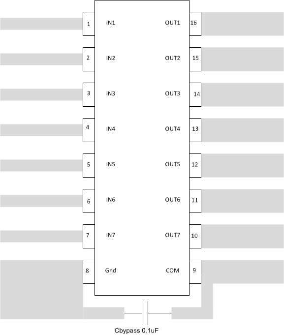
Thin traces can be used on the input due to the low current logic that is typically used to drive ULN2003LV. Take care to separate the input channels as much as possible, as to eliminate cross-talk. Thick traces are recommended for the output, in order to drive high currents that may be needed. Wire thickness can be determined by the trace material's current density and desired drive current. Since all of the channels currents return to a common ground, it is best to size that trace width to be very wide. Some applications require up to 1 A.
10.2 Layout Example
 Figure 14. Layout Example Recommendation
10.3 On-Chip Power Dissipation
Use Equation 3 to calculate ULN2003LV on-chip power dissipation PD:

where
- N is the number of channels active together.
- VOLi is the OUTi pin voltage for the load current ILi.
10.4 Thermal Considerations
TI recommends to limit ULN2003LV IC’s die junction temperature to less than 125°C. The IC junction temperature is directly proportional to the on-chip power dissipation. Use the following equation to calculate the maximum allowable on-chip power dissipation for a target IC junction temperature:

where
- TJ(MAX) is the target maximum junction temperature.
- TA is the operating ambient temperature.
- RθJA is the package junction to ambient thermal resistance.
10.4.1 Improving Package Thermal Performance
The package RθJA value under standard conditions on a High-K board is listed in the Dissipation Ratings. RθJA value depends on the PCB layout. An external heat sink and/or a cooling mechanism, like a cold air fan, can help reduce RθJA and thus improve device thermal capabilities. Refer to TI’s design support web page at www.ti.com/thermal for a general guidance on improving device thermal performance.