ZHCS846B April 2012 – June 2015 ULN2003LV
PRODUCTION DATA.
6 Specifications
6.1 Absolute Maximum Ratings
Specified at TJ = –40°C to 125°C unless otherwise noted.(1)| MIN | MAX | UNIT | |||
|---|---|---|---|---|---|
| VIN | Pins IN1- IN7 to GND voltage | –0.3 | 5.5 | V | |
| VOUT | Pins OUT1 – OUT7 to GND voltage | 8 | V | ||
| VCOM | Pin COM to GND voltage | 8 | V | ||
| IGND | Maximum GND-pin continuous current (TJ > +125°C) | 700 | mA | ||
| Maximum GND-pin continuous current (TJ < +100°C) | 1.0 | A | |||
| PD | Total device power dissipation at TA = 85°C | 16 Pin - SOIC | 0.58 | W | |
| 16 Pin -TSSOP | 0.45 | W | |||
| TA | Operating free-air ambient temperature | –40 | 85 | °C | |
| TJ | Operating virtual junction temperature | –55 | 150 | °C | |
| Tstg | Storage temperature | –55 | 150 | °C | |
(1) Stresses beyond those listed under Absolute Maximum Ratings may cause permanent damage to the device. These are stress ratings only, which do not imply functional operation of the device at these or any other conditions beyond those indicated under Recommended Operating Conditions. Exposure to absolute-maximum-rated conditions for extended periods may affect device reliability.
6.2 ESD Ratings
| VALUE | UNIT | |||
|---|---|---|---|---|
| V(ESD) | Electrostatic discharge | Human body model (HBM), per ANSI/ESDA/JEDEC JS-001(1) | ±2000 | V |
| Charged-device model (CDM), per JEDEC specification JESD22-C101(2) | ±500 | |||
(1) JEDEC document JEP155 states that 500-V HBM allows safe manufacturing with a standard ESD control process.
(2) JEDEC document JEP157 states that 250-V CDM allows safe manufacturing with a standard ESD control process.
6.3 Recommended Operating Conditions
over operating free-air temperature range (unless otherwise noted)| MIN | MAX | UNIT | |||
|---|---|---|---|---|---|
| VOUT | Channel off-state output pullup voltage | 8 | V | ||
| VCOM | COM pin voltage | 8 | V | ||
| IOUT(ON) | Per channel continuous sink current | VINx = 3.3 V | 100(1) | mA | |
| VINx = 5.0 V | 140(1) | ||||
| TJ | Operating junction temperature | –40 | 125 | ºC | |
(1) Refer to Absolute Maximum Ratings for TJ dependent absolute maximum GND-pin current
6.4 Thermal Information
| THERMAL METRIC(1) | ULN2003LV | UNIT | ||
|---|---|---|---|---|
| D (SOIC) | PW (TSSOP) | |||
| 16 PINS | 16 PINS | |||
| RθJA | Junction-to-ambient thermal resistance | 112 | 142 | °C/W |
| RθJC(top) | Junction-to-case (top) thermal resistance | 69 | 74 | °C/W |
| RθJB | Junction-to-board thermal resistance | 69 | 87 | °C/W |
| ψJT | Junction-to-top characterization parameter | 33 | 22 | °C/W |
| ψJB | Junction-to-board characterization parameter | 69 | 87 | °C/W |
(1) For more information about traditional and new thermal metrics, see the Semiconductor and IC Package Thermal Metrics application report, SPRA953.
6.5 Electrical Characteristics
Specified over the recommended junction temperature range TJ = –40°C to 125°C unless otherwise noted. Typical values are at TJ = 25°C.| PARAMETER | TEST CONDITIONS | MIN | TYP | MAX | UNIT | |
|---|---|---|---|---|---|---|
| INPUTS IN1 THROUGH IN7 PARAMETERS | ||||||
| VI(ON) | IN1–IN7 logic high input voltage | Vpull-up = 3.3 V, Rpullup = 1 kΩ, IOUTX = 3.2 mA | 1.65 | V | ||
| VI(OFF) | IN1–IN7 logic low input voltage | Vpullup = 3.3 V, Rpullup = 1 kΩ, (IOUTX = <5 µA) |
0.4 | 0.6 | V | |
| II(ON) | IN1–IN7 ON state input current | Vpullup = 3.3 V, VINx = 3.3 V | 12 | 25 | µA | |
| II(OFF) | IN1–IN7 OFF state input leakage | Vpullup = 3.3 V, VINx = 0 V | 250 | nA | ||
| OUTPUTS OUT1 THROUGH OUT7 PARAMETERS | ||||||
| VOL(VCE-SAT) | OUT1–OUT7 low-level output voltage | VINX = 3.3 V, IOUTX = 50 mA | 0.17 | 0.24 | V | |
| VINX = 3.3 V, IOUTX = 100 mA | 0.36 | 0.49 | ||||
| VINX = 5.0 V, IOUTX = 100 mA | 0.26 | 0.42 | ||||
| VINX = 5.0 V, IOUTX = 140 mA | 0.40 | |||||
| IOUT(ON) | OUT1–OUT7 ON-state continuous current(1) (2) at VOUTX = 0.4V | VINX = 3.3 V, VOUTX = 0.4 V | 80 | 100 | mA | |
| VINX = 5.0 V, VOUTX = 0.4 V | 95 | 140 | ||||
| IOUT(OFF)(ICEX) | OUT1–OUT7 OFF-state leakage current | VINX = 0 V, VOUTX = VCOM = 8 V | 0.17 | µA | ||
| FREE-WHEELING DIODE PARAMETERS(3)(4) | ||||||
| VF | Forward voltage drop | IF-peak = 140 mA, VF = VOUTx – VCOM, | 1.2 | V | ||
| IF-peak | Diode peak forward current | 140 | mA | |||
(1) The typical continuous current rating is limited by VOL= 0.4V. Whereas, absolute maximum operating continuous current may be limited by the Thermal Performance.parameters listed in the Dissipation Rating Table and other Reliability parameters listed in the Recommended Operating ConditionsTable.
(2) Refer to the Absolute Maximum Ratings table for TJ dependent absolute maximum GND-pin current.
(3) Not rated for continuous current operation – for higher reliability use an external freewheeling diode for inductive loads resulting in more than specified maximum free-wheeling. diode peak current across various temperature conditions
(4) Specified by design only.
6.6 Switching Characteristics
over operating free-air temperature range (unless otherwise noted)(1)(2)| PARAMETER | TEST CONDITIONS | MIN | TYP | MAX | UNIT | |
|---|---|---|---|---|---|---|
| tPHL | OUT1–OUT7 logic high propagation delay | VINX = 3.3V, Vpull-up = 3.3 V, Rpull-up = 50 Ω | 25 | ns | ||
| VINX = 5.0V, Vpull-up = 5 V, Rpull-up = 1 kΩ | 15 | |||||
| tPLH | OUT1–OUT7 logic low propagation delay | VINX = 3.3V, Vpull-up = 3.3 V, Rpull-up = 50 Ω | 45 | ns | ||
| VINX = 5.0V, Vpull-up = 5 V, Rpull-up = 1kΩ | 80 | |||||
| RPD | IN1–IN7 input pull-down Resistance | 210 | 300 | 390 | kΩ | |
| ζ | IN1–IN7 Input filter time constant | 9 | ns | |||
| COUT | OUT1–OUT7 output capacitance | VINX = 3.3 V, VOUTX = 0.4 V | 15 | pF | ||
(1) Rise and Fall propagation delays, tPHL and tPLH, are measured between 50% values of the input and the corresponding output signal amplitude transition.
(2) Specified by design only.
6.7 Dissipation Ratings
See (1)(3)| BOARD | PACKAGE | RθJC | RθJA(2) | DERATING FACTOR ABOVE TA = 25ºC | TA < 25°C | TA = 70°C | TA = 85°C |
|---|---|---|---|---|---|---|---|
| High-K | 16-Pin SOIC | 69°C/W | 112°C/W | 8.88 mW/ºC | 1.11 W | 0.71 W | 0.58 W |
| High-K | 16-Pin TSSOP | 74°C/W | 142°C/W | 7.11 mW/ºC | 0.88 W | 0.56 W | 0.45 W |
(1) Maximum dissipation values for retaining device junction temperature of 150°C
(2) Operating at the absolute TJ-max of 150°C can affect reliability– for higher reliability it is recommended to ensure TJ < 125°C
(3) Refer to TI’s design support web page at www.ti.com/thermal for improving device thermal performance
6.8 Typical Characteristics
TA = +25ºC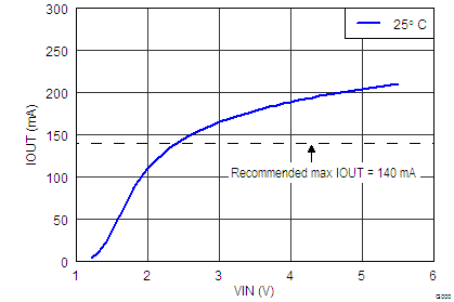 Figure 1. Load Current 1-Channel; VOL=0.4V
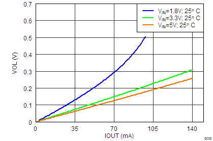 Figure 3. VOL versus IOUT VIN = 1.8V, 3.3V, 5.0V
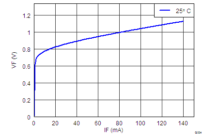 Figure 5. Freewheeling Diode VF vs IF
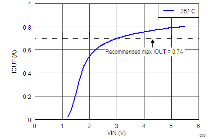 Figure 2. Load Current 7-Channels in Parallel; VOL=0.4V
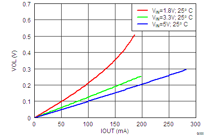 Figure 4. VOL versus IOUT 2-Channels in Parallel; VOL=0.4V