ZHCSC42J July 2013 – October 2014 WL1801MOD , WL1805MOD , WL1831MOD , WL1835MOD
PRODUCTION DATA.
- 1器件概述
- 2修订历史记录
- 3Device Comparison
- 4Terminal Configuration and Functions
-
5Specifications
- 5.1 Absolute Maximum Ratings
- 5.2 Handling Ratings
- 5.3 Power-On Hours (POH)
- 5.4 Recommended Operating Conditions
- 5.5 External Digital Slow Clock Requirements
- 5.6 Thermal Characteristics
- 5.7 WLAN Performance
- 5.8 Bluetooth Performance
- 5.9 Bluetooth LE Performance
- 5.10 Bluetooth-BLE Dynamic Currents
- 5.11 Bluetooth LE Currents
- 5.12
Timing and Switching Characteristics
- 5.12.1 Power Management
- 5.12.2 Power-Up and Shut-Down States
- 5.12.3 Chip Top-level Power-Up Sequence
- 5.12.4 WLAN Power-Up Sequence
- 5.12.5 Bluetooth-BLE Power-Up Sequence
- 5.12.6 WLAN SDIO Transport Layer
- 5.12.7 HCI UART Shared Transport Layers for All Functional Blocks (Except WLAN)
- 5.12.8 Bluetooth Codec-PCM (Audio) Timing Specifications
- 6Detailed Description
- 7Applications and Implementation
- 8Device and Documentation Support
- 9Mechanical Packaging and Orderable Information
4 Terminal Configuration and Functions
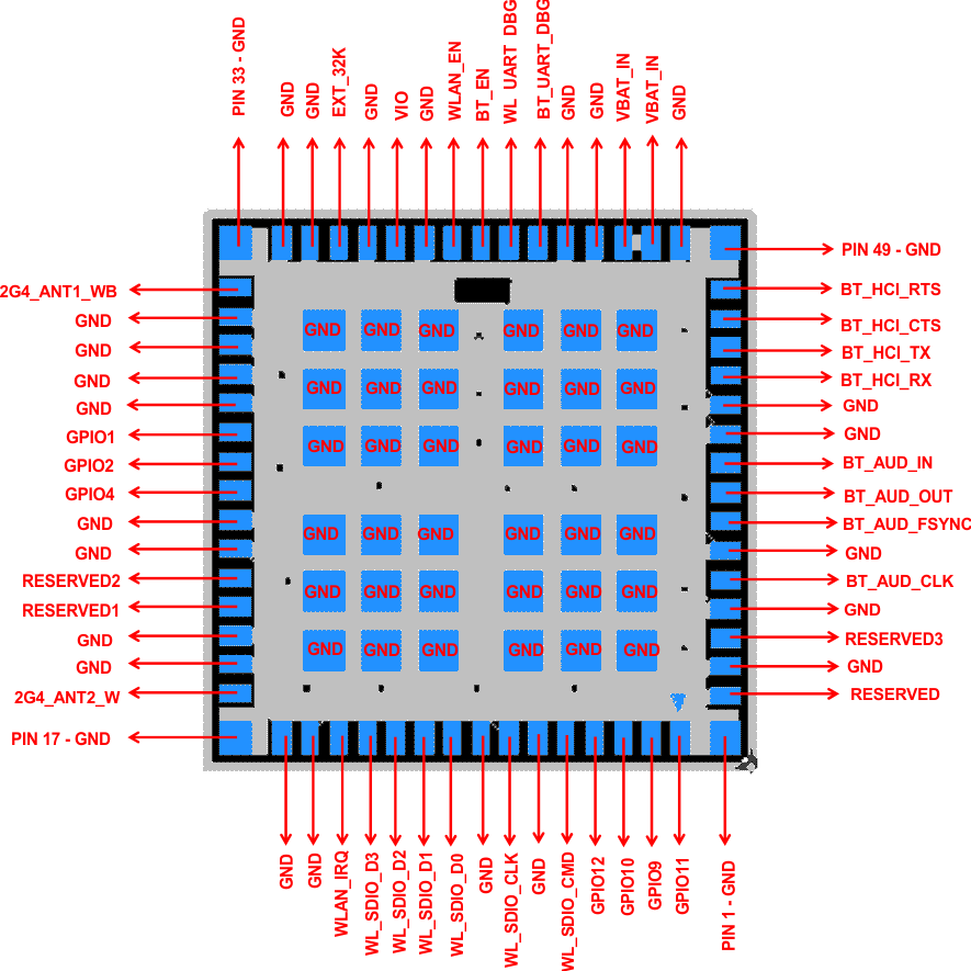
Figure 4-1 shows the pin assignments for the 100-pin MOC package.
Figure 4-2 shows the outline of the 100-pin MOC package.

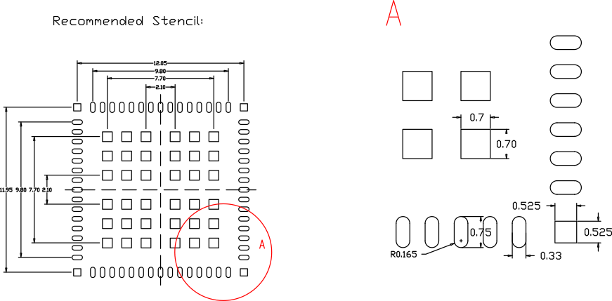
NOTE: 1. Module size: 13.4 x 13.3 mm
2. Pad size: 0.75 x 0.40 mm
3. Pitch: 0.7 mm
Figure 4-2 Outline of 100-Pin MOC Package
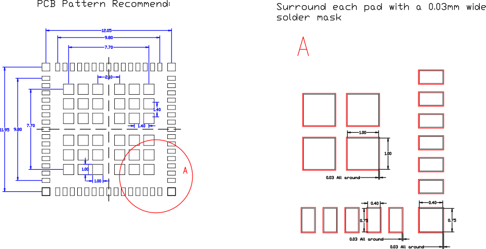
Figure 4-3 shows the outline of the recommended PCB pattern for the 100-pin MOC package.
4.1 Pin Description
Table 4-1 describes the module pins.
Table 4-1 Pin Description
| PIN NAME | PIN | TYPE/DIR | SHUTDOWN STATE | AFTER POWER UP(2) | VOLTAGE LEVEL | CONNECTIVITY(3) | DESCRIPTION | |||
|---|---|---|---|---|---|---|---|---|---|---|
| 1801 | 1805 | 1831 | 1835 | |||||||
| Clocks and Reset SIgnals | ||||||||||
| WL_SDIO_CLK_1V8 | 8 | I | Hi-Z | Hi-Z | 1.8 V | v | v | v | v | WLAN SDIO clock. Must be driven by the host. |
| EXT_32K | 36 | ANA | – | v | v | v | v | Input sleep clock: 32.768 kHz | ||
| WLAN_EN | 40 | I | PD | PD | 1.8 V | v | v | v | v | Mode setting: high = enable |
| BT_EN | 41 | I | PD | PD | 1.8 V | x | x | v | v | Mode setting: high = enable |
| Power-Management Signals | ||||||||||
| VIO_IN | 38 | POW | PD | PD | 1.8 V | v | v | v | v | Connect to 1.8-V external VIO |
| VBAT_IN | 46 | POW | VBAT | v | v | v | v | Power supply input, 2.9 to 4.8 V | ||
| VBAT_IN | 47 | POW | VBAT | v | v | v | v | Power supply input, 2.9 to 4.8 V | ||
| TI Reserved | ||||||||||
| GPIO11 | 2 | I/O | PD | PD | 1.8 V | v | v | v | v | Reserved for future use. NC if not used. |
| GPIO9 | 3 | I/O | PD | PD | 1.8 V | v | v | v | v | Reserved for future use. NC if not used. |
| GPIO10 | 4 | I/O | PU | PU | 1.8 V | v | v | v | v | Reserved for future use. NC if not used. |
| GPIO12 | 5 | I/O | PU | PU | 1.8 V | v | v | v | v | Reserved for future use. NC if not used. |
| RESERVED1 | 21 | I | PD | PD | 1.8 V | x | x | x | x | Reserved for future use. NC if not used. |
| RESERVED2 | 22 | I | PD | PD | 1.8 V | x | x | x | x | Reserved for future use. NC if not used. |
| GPIO4 | 25 | I/O | PD | PD | 1.8 V | v | v | v | v | Reserved for future use. NC if not used. |
| RESERVED3 | 62 | O | PD | PD | 1.8 V | x | x | x | x | Reserved for future use. NC if not used. |
| RESERVED | 64 | GND | – | v | v | v | v | Reserved for future use. NC if not used. | ||
| WLAN Functional Block: Int Signals | ||||||||||
| WL_SDIO_CMD_1V8 | 6 | I/O | Hi-Z | Hi-Z | 1.8 V | v | v | v | v | WLAN SDIO command in(1) |
| WL_SDIO_D0_1V8 | 10 | I/O | Hi-Z | Hi-Z | 1.8 V | v | v | v | v | WLAN SDIO data bit 0(1) |
| WL_SDIO_D1_1V8 | 11 | I/O | Hi-Z | Hi-Z | 1.8 V | v | v | v | v | WLAN SDIO data bit 1(1) |
| WL_SDIO_D2_1V8 | 12 | IO | Hi-Z | Hi-Z | 1.8 V | v | v | v | v | WLAN SDIO data bit 2(1) |
| WL_SDIO_D3_1V8 | 13 | I/O | Hi-Z | PU | 1.8 V | v | v | v | v | WLAN SDIO data bit 3. Changes state to PU at WL_EN or BT_EN assertion for card detects. Later disabled by software during initialization. (1) |
| WL_IRQ_1V8 | 14 | O | PD | 0 | 1.8 V | v | v | v | v | SDIO available, interrupt out. Active high. (For WL_RS232_TX/RX pullup is at power up.) Set to rising edge (active high) on power up. The Wi-Fi interrupt line can be configured by the driver according to the IRQ configuration (polarity/level/edge). |
| GPIO2 | 26 | I/O | PD | PD | 1.8 V | v | v | v | v | WL_RS232_RX (when WLAN_IRQ = 1 at power up) |
| 2G4_ANT2_W | 18 | ANA | – | x | v | x | v | 2.4G ant2 TX, RX | ||
| GPIO1 | 27 | I/O | PD | PD | 1.8 V | v | v | v | v | WL_RS232_TX (when WLAN_IRQ = 1 at power up) |
| 2G4_ANT1_WB | 32 | ANA | – | v | v | v | v | 2.4G ant1 TX, RX | ||
| WL_UART_DBG | 42 | O | PU | PU | 1.8 V | v | v | v | v | Option: WLAN logger |
| Bluetooth Functional Block: Int Signals | ||||||||||
| BT_UART_DBG | 43 | O | PU | PU | 1.8 V | x | x | v | v | Option: Bluetooth logger |
| BT_HCI_RTS_1V8 | 50 | O | PU | PU | 1.8 V | x | x | v | v | UART RTS to host. NC if not used. |
| BT_HCI_CTS_1V8 | 51 | I | PU | PU | 1.8 V | x | x | v | v | UART CTS from host. NC if not used. |
| BT_HCI_TX_1V8 | 52 | O | PU | PU | 1.8 V | x | x | v | v | UART TX to host. NC if not used. |
| BT_HCI_RX_1V8 | 53 | I | PU | PU | 1.8 V | x | x | v | v | UART RX from host. NC if not used. |
| BT_AUD_IN | 56 | I | PD | PD | 1.8 V | x | x | v | v | Bluetooth PCM/I2S bus. Data in. NC if not used. |
| BT_AUD_OUT | 57 | O | PD | PD | 1.8 V | x | x | v | v | Bluetooth PCM/I2S bus. Data out. NC if not used. |
| BT_AUD_FSYNC | 58 | I/O | PD | PD | 1.8 V | x | x | v | v | Bluetooth PCM/I2S bus. Frame sync. NC if not used. |
| BT_AUD_CLK | 60 | I/O | PD | PD | 1.8 V | x | x | v | v | Bluetooth PCM/I2S bus. NC if not used. |
| Ground Pins | ||||||||||
| GND | 1, 7, 9, 15, 16, 17, 19, 20, 23, 24, 28, 29, 30, 31, 33, 34, 35, 37, 39, 44, 45, 48, 49, 54, 55, 59, 61, 63, G1-G36 | GND | – | v | v | v | v | |||
(1) Host must provide PU using a 10-K resistor for all non-CLK SDIO signals.
(2) PU = pullup; PD = pulldown.
(3) v = connect; x = no connect.

