ZHCSC42J July 2013 – October 2014 WL1801MOD , WL1805MOD , WL1831MOD , WL1835MOD
PRODUCTION DATA.
- 1器件概述
- 2修订历史记录
- 3Device Comparison
- 4Terminal Configuration and Functions
-
5Specifications
- 5.1 Absolute Maximum Ratings
- 5.2 Handling Ratings
- 5.3 Power-On Hours (POH)
- 5.4 Recommended Operating Conditions
- 5.5 External Digital Slow Clock Requirements
- 5.6 Thermal Characteristics
- 5.7 WLAN Performance
- 5.8 Bluetooth Performance
- 5.9 Bluetooth LE Performance
- 5.10 Bluetooth-BLE Dynamic Currents
- 5.11 Bluetooth LE Currents
- 5.12
Timing and Switching Characteristics
- 5.12.1 Power Management
- 5.12.2 Power-Up and Shut-Down States
- 5.12.3 Chip Top-level Power-Up Sequence
- 5.12.4 WLAN Power-Up Sequence
- 5.12.5 Bluetooth-BLE Power-Up Sequence
- 5.12.6 WLAN SDIO Transport Layer
- 5.12.7 HCI UART Shared Transport Layers for All Functional Blocks (Except WLAN)
- 5.12.8 Bluetooth Codec-PCM (Audio) Timing Specifications
- 6Detailed Description
- 7Applications and Implementation
- 8Device and Documentation Support
- 9Mechanical Packaging and Orderable Information
5 Specifications
5.1 Absolute Maximum Ratings(1)
over operating free-air temperature range (unless otherwise noted)| PARAMETER | VALUE | UNIT | |
|---|---|---|---|
| VBAT | 4.8(2) | V | |
| VIO | –0.5 to 2.1 | V | |
| Input voltage to analog pins | –0.5 to 2.1 | V | |
| Input voltage limits (CLK_IN) | –0.5 to VDD_IO | V | |
| Input voltage to all other pins | –0.5 to (VDD_IO + 0.5 V) | V | |
| Operating ambient temperature range | –20 to +70(3) | °C | |
5.2 Handling Ratings
| MIN | MAX | UNIT | ||
|---|---|---|---|---|
| Tstg | Storage temperature range | –40 | +85 | °C |
| ESD stress voltage(1) | Human body model (HBM)(2) | –1000 | +1000 | V |
| Charged device model (CDM)(3) | –250 | +250 |
5.3 Power-On Hours (POH)
| OPERATING JUNCTION TEMPERATURE (°C) | POH |
|---|---|
| 125 | 15,000 |
| 120 | 20,000 |
| 115 | 27,000 |
| 110 | 37,000 |
| 105 | 50,000 |
5.4 Recommended Operating Conditions
over operating free-air temperature range (unless otherwise noted)| MIN | NOM | MAX | UNIT | |||
|---|---|---|---|---|---|---|
| VBAT(2) | DC supply range for all modes | 2.9 | 4.8 | V | ||
| 1.8-V I/O ring power supply voltage | 1.62 | 1.95 | V | |||
| VIH | I/O high-level input voltage | 0.65 x VDD_IO | VDD_IO | V | ||
| VIL | I/O low-level input voltage | 0 | 0.35 × VDD_IO | V | ||
| VIH_EN | Enable inputs high-level input voltage | 1.365 | VDD_IO | V | ||
| VIL_EN | Enable inputs low-level input voltage | 0 | 0.4 | V | ||
| VOH | High-level output voltage | @ 4 mA | VDD_IO –0.45 | VDD_IO | V | |
| VOL | Low-level output voltage | @ 4 mA | 0 | 0.45 | V | |
| Tr,Tf | Input transitions time Tr,Tf from 10% to 90% (digital I/O)(1) | 1 | 10 | ns | ||
| Tr | Output rise time from 10% to 90% (digital pins)(1) | CL < 25 pF | 5.3 | ns | ||
| Tf | Output fall time from 10% to 90% (digital pins)(1) | CL < 25 pF | 4.9 | ns | ||
| Ambient operating temperature | –20 | 70 | ºC | |||
| Maximum power dissipation | WLAN operation | 2.8 | W | |||
| Bluetooth operation | 0.2 | |||||
5.5 External Digital Slow Clock Requirements
The supported digital slow clock is 32.768 kHz digital (square wave). All core functions share a single input.| PARAMETER | CONDITION | SYMBOL | MIN | TYP | MAX | UNIT |
|---|---|---|---|---|---|---|
| Input slow clock frequency | 32768 | Hz | ||||
| Input slow clock accuracy (Initial + temp + aging) | WLAN, Bluetooth | ±250 | ppm | |||
| Input transition time Tr,Tf (10% to 90%) | Tr,Tf | 200 | ns | |||
| Frequency input duty cycle | 15 | 50 | 85 | % | ||
| Input voltage limits | Square wave, DC-coupled | Vih | 0.65 x VDD_IO | VDD_IO | Vpeak | |
| Vil | 0 | 0.35 x VDD_IO | ||||
| Input impedance | 1 | MΩ | ||||
| Input capacitance | 5 | pF |
5.6 Thermal Characteristics
| AIR FLOW | ||
|---|---|---|
| NAME | DESCRIPTION | FCBGA (°C/W)(1) |
| θJC | Junction to case | 12.7 |
| θJB | Junction to board | 13.6 |
| θJA | Junction to free air(2) | 20.5 |
| φJB | Junction to board | 8.7 |
5.7 WLAN Performance
All RF and performance numbers are aligned to the module pin.
5.7.1 WLAN 2.4-GHz Receiver Characteristics
over operating free-air temperature range (unless otherwise noted)
| PARAMETER | CONDITION | MIN | TYP | MAX | UNIT |
|---|---|---|---|---|---|
| Operation frequency range | 2400 to 2480 | 2400 | 2480 | MHz | |
| Sensitivity: 20-MHz bandwidth. At < 10% PER limit | 1 Mbps DSSS | –96.3 | dBm | ||
| 2 Mbps DSSS | –93.2 | ||||
| 5.5 Mbps CCK | –90.6 | ||||
| 11 Mbps CCK | –87.9 | ||||
| 6 Mbps OFDM | –92.0 | ||||
| 9 Mbps OFDM | –90.4 | ||||
| 12 Mbps OFDM | –89.5 | ||||
| 18 Mbps OFDM | –87.2 | ||||
| 24 Mbps OFDM | –84.1 | ||||
| 36 Mbps OFDM | –80.7 | ||||
| 48 Mbps OFDM | –76.5 | ||||
| 54 Mbps OFDM | –74.9 | ||||
| MCS0 MM 4K | –90.4 | ||||
| MCS1 MM 4K | –87.6 | ||||
| MCS2 MM 4K | –85.9 | ||||
| MCS3 MM 4K | –82.8 | ||||
| MCS4 MM 4K | –79.4 | ||||
| MCS5 MM 4K | –75.2 | ||||
| MCS6 MM 4K | –73.5 | ||||
| MCS7 MM 4K | –72.4 | ||||
| MCS0 MM 4K 40 MHz | –86.7 | ||||
| MCS7 MM 4K 40 MHz | –67.0 | ||||
| MCS0 MM 4K MRC | –92.7 | ||||
| MCS7 MM 4K MRC | –75.2 | ||||
| MCS13 MM 4K | –73.7 | ||||
| MCS14 MM 4K | –72.3 | ||||
| MCS15 MM 4K | –71.0 | ||||
| Max Input Level At < 10% PER limit | OFDM (11g/n) | –19 | –9 | dBm | |
| DSSS | –4 | –0 | dBm | ||
| Adjacent channel rejection: Sensitivity level +3 dB for OFDM; Sensitivity level +6 dB for 11b | 2 Mbps DSSS | 42.7 | dB | ||
| 11 Mbps CCK | 37.9 | dB | |||
| 54 Mbps OFDM | 2.0 | dB |
5.7.2 WLAN 2.4-GHz Transmitter Power
over operating free-air temperature range (unless otherwise noted)
| PARAMETER | CONDITION | MIN | TYP | MAX | UNIT |
|---|---|---|---|---|---|
| RF_IO2_BG_WL pin 2.4-GHz SISO | |||||
| Output Power: Maximum RMS output power measured at 1 dB from IEEE spectral mask or EVM(1) | 1 Mbps DSSS | 17.3 | dBm | ||
| 2 Mbps DSSS | 17.3 | ||||
| 5.5 Mbps CCK | 17.3 | ||||
| 11 Mbps CCK | 17.3 | ||||
| 6 Mbps OFDM | 17.1 | ||||
| 9 Mbps OFDM | 17.1 | ||||
| 12 Mbps OFDM | 17.1 | ||||
| 18 Mbps OFDM | 17.1 | ||||
| 24 Mbps OFDM | 16.2 | ||||
| 36 Mbps OFDM | 15.3 | ||||
| 48 Mbps OFDM | 14.6 | ||||
| 54 Mbps OFDM | 13.8 | ||||
| MCS0 MM | 16.1 | ||||
| MCS1 MM | 16.1 | ||||
| MCS2 MM | 16.1 | ||||
| MCS3 MM | 16.1 | ||||
| MCS4 MM | 15.3 | ||||
| MCS5 MM | 14.6 | ||||
| MCS6 MM | 13.8 | ||||
| MCS7 MM(2) | 12.6 | ||||
| MCS0 MM 40 MHz | 14.8 | ||||
| MCS7 MM 40 MHz | 11.3 | ||||
| 2G4_ANT2_W + 2G4_ANT1_WB 2.4-GHz MIMO | |||||
| MCS12 (WL18x5) | 18.5 | dBm | |||
| MCS13 (WL18x5) | 17.4 | ||||
| MCS14 (WL18x5) | 14.5 | ||||
| MCS15 (WL18x5) | 13.4 | ||||
| 2G4_ANT2_W + 2G4_ANT1_WB Pins | |||||
| Operation frequency range | 2412 | 2484 | MHz | ||
| Return loss | –10.0 | dB | |||
| Reference input impedance | 50.0 | Ω | |||
5.7.3 WLAN Currents
5.8 Bluetooth Performance
All RF and performance numbers are aligned to the module pin.
5.8.1 Bluetooth BR, EDR Receiver Characteristics—In-Band Signals
over operating free-air temperature range (unless otherwise noted)
| PARAMETER | CONDITION | MIN | TYP | MAX | UNIT | |
|---|---|---|---|---|---|---|
| Bluetooth BR, EDR operation frequency range | 2402 | 2480 | MHz | |||
| Bluetooth BR, EDR channel spacing | 1 | MHz | ||||
| Bluetooth BR, EDR input impedance | 50 | Ω | ||||
| Bluetooth BR, EDR sensitivity(1)
dirty TX on |
BR, BER = 0.1% | –92.2 | dBm | |||
| EDR2, BER = 0.01% | –91.7 | dBm | ||||
| EDR3, BER = 0.01% | –84.7 | dBm | ||||
| Bluetooth EDR BER floor at sensitivity + 10 dB Dirty TX off (for 1,600,000 bits) |
EDR2 | 1e-6 | ||||
| EDR3 | 1e-6 | |||||
| Bluetooth BR, EDR maximum usable input power | BR, BER = 0.1% | –5.0 | dBm | |||
| EDR2, BER = 0.1% | –15.0 | dBm | ||||
| EDR3, BER = 0.1% | –15.0 | dBm | ||||
| Bluetooth BR intermodulation | Level of interferers for n = 3, 4, and 5 | –36.0 | –30.0 | dBm | ||
| Bluetooth BR, EDR C/I performance Numbers show wanted signal-to-interfering-signal ratio. Smaller numbers indicate better C/I performances (Image frequency = –1 MHz) |
BR, co-channel | 10 | dB | |||
| EDR, co-channel | EDR2 | 12 | dB | |||
| EDR3 | 20 | dB | ||||
| BR, adjacent ±1 MHz | –3.0 | dB | ||||
| EDR, adjacent ±1 MHz, (image) | EDR2 | –3.0 | dB | |||
| EDR3 | 2.0 | dB | ||||
| BR, adjacent +2 MHz | –33.0 | dB | ||||
| EDR, adjacent +2 MHz | EDR2 | –33.0 | dB | |||
| EDR3 | –28.0 | dB | ||||
| BR, adjacent –2 MHz | –20.0 | dB | ||||
| EDR, adjacent –2 MHz | EDR2 | –20.0 | dB | |||
| EDR3 | –13.0 | dB | ||||
| BR, adjacent ≥Ι±3Ι MHz | –42.0 | dB | ||||
| EDR, adjacent ≥Ι±3Ι MHz | EDR2 | –42.0 | dB | |||
| EDR3 | –36.0 | dB | ||||
| Bluetooth BR, EDR RF return loss | –10.0 | dB | ||||
5.8.2 Bluetooth Transmitter, BR
over operating free-air temperature range (unless otherwise noted)
| PARAMETER | MIN | TYP | MAX | UNIT | |
|---|---|---|---|---|---|
| BR RF output power(1) | VBAT ≥ 3 V | 12.7 | dBm | ||
| VBAT < 3 V | 7.2 | dBm | |||
| BR gain control range | 30.0 | dB | |||
| BR power control step | 5.0 | dB | |||
| BR adjacent channel power |M-N| = 2 | –43.0 | dBm | |||
| BR adjacent channel power |M-N| > 2 | –48.0 | dBm | |||
5.8.3 Bluetooth Transmitter, EDR
over operating free-air temperature range (unless otherwise noted)
| PARAMETER | MIN | TYP | MAX | UNIT | |
|---|---|---|---|---|---|
| EDR output power(1) | VBAT ≥ 3 V | 7.2 | dBm | ||
| VBAT < 3 V | 5.2 | ||||
| EDR relative power | dB | ||||
| EDR gain control range | 30 | dB | |||
| EDR power control step | 5 | dB | |||
| EDR adjacent channel power |M-N| = 1 | –36 | dBc | |||
| EDR adjacent channel power |M-N| = 2 | –30 | dBm | |||
| EDR adjacent channel power |M-N| > 2 | –42 | dBm | |||
5.8.4 Bluetooth Modulation, BR
over operating free-air temperature range (unless otherwise noted)
| CHARACTERISTICS | CONDITION(1) | MIN | TYP | MAX | UNIT | |
|---|---|---|---|---|---|---|
| BR –20 dB bandwidth | 925 | 995 | kHz | |||
| BR modulation characteristics | ∆f1avg | Mod data = 4 1s, 4 0s: 111100001111... | 145 | 160 | 170 | kHz |
| ∆f2max ≥ limit for at least 99.9% of all Δf2max | Mod data = 1010101... | 120 | 130 | kHz | ||
| ∆f2avg, ∆f1avg | 85 | 88 | % | |||
| BR carrier frequency drift | One slot packet | –25 | 25 | kHz | ||
| Three and five slot packet | –35 | 35 | kHz | |||
| BR drift rate | lfk+5 – fkl , k = 0 …. max | 15 | kHz/50 µs | |||
| BR initial carrier frequency tolerance(2) | f0–fTX | ±75 | ±75 | kHz | ||
5.8.5 Bluetooth Modulation, EDR
over operating free-air temperature range (unless otherwise noted)
| PARAMETER(1) | CONDITION | MIN | TYP | MAX | UNIT |
|---|---|---|---|---|---|
| EDR carrier frequency stability | –5 | 5 | kHz | ||
| EDR initial carrier frequency tolerance(2) | ±75 | ±75 | kHz | ||
| EDR RMS DEVM | EDR2 | 4 | 15 | % | |
| EDR3 | 4 | 10 | % | ||
| EDR 99% DEVM | EDR2 | 30 | % | ||
| EDR3 | 20 | % | |||
| EDR peak DEVM | EDR2 | 9 | 25 | % | |
| EDR3 | 9 | 18 | % |
5.9 Bluetooth LE Performance
All RF and performance numbers are aligned to the module pin.
5.9.1 Bluetooth LE Receiver Characteristics – In-Band Signals
over operating free-air temperature range (unless otherwise noted)
| PARAMETER | CONDITION(2) | MIN | TYP | MAX | UNIT |
|---|---|---|---|---|---|
| Bluetooth LE operation frequency range | 2402 | 2480 | MHz | ||
| Bluetooth LE channel spacing | 2 | MHz | |||
| Bluetooth LE input impedance | 50 | Ω | |||
| Bluetooth LE sensitivity(1)
Dirty TX on |
–92.2 | dBm | |||
| Bluetooth LE maximum usable input power | –5 | dBm | |||
| Bluetooth LE intermodulation characteristics | Level of interferers. For n = 3, 4, 5 |
–36 | –30 | dBm | |
| Bluetooth LE C/I performance. Note: Numbers show wanted signal-to-interfering-signal ratio. Smaller numbers indicate better C/I performance. |
LE, co-channel | 12 | dB | ||
| LE, adjacent ±1 MHz | 0 | ||||
| LE, adjacent +2 MHz | –38 | ||||
| LE, adjacent –2 MHz | –15 | ||||
| Image = –1 MHz | LE, adjacent ≥ |±3|MHz | –40 |
5.9.2 Bluetooth LE Transmitter Characteristics
over operating free-air temperature range (unless otherwise noted)
| PARAMETER | MIN | TYP | MAX | UNIT | |
|---|---|---|---|---|---|
| Bluetooth LE RF output power(1) | VBAT ≥ 3 V | 10.0 | dBm | ||
| VBAT < 3 V | 7.2 | dBm | |||
| Bluetooth LE adjacent channel power |M-N| = 2 | –51.0 | dBm | |||
| Bluetooth LE adjacent channel power |M-N| > 2 | –54.0 | dBm |
5.9.3 Bluetooth LE Modulation Characteristics
over operating free-air temperature range (unless otherwise noted)
| CHARACTERISTICS | CONDITION(1) | MIN | TYP | MAX | UNIT | |
|---|---|---|---|---|---|---|
| Bluetooth LE modulation characteristics | ∆f1avg | Mod data = 4 1s, 4 0s: 111100001111... | 240 | 250 | 260 | kHz |
| ∆f2max ≥ limit for at least 99.9% of all Δf2max | Mod data = 1010101... | 195 | 215 | kHz | ||
| ∆f2avg, ∆f1avg | 85 | 90 | % | |||
| Bluetooth LE carrier frequency drift | lf0 – fnl , n = 2,3 …. K | –25 | 25 | kHz | ||
| Bluetooth LE drift rate | lf1 – f0l and lfn – fn-5l ,n = 6,7…. K | 15 | kHz/50 µs | |||
| LE initial carrier frequency tolerance(2) | fn – fTX | ±75 | ±75 | kHz | ||
5.10 Bluetooth-BLE Dynamic Currents
Current is measured at output power as follows:
- BR at 12.7 dBm
- EDR at 7.2 dBm
| USE CASE(1)(2) | TYP | UNIT |
|---|---|---|
| BR voice HV3 + sniff | 11.6 | mA |
| EDR voice 2-EV3 no retransmission + sniff | 5.9 | mA |
| Sniff 1 attempt 1.28 s | 178.0 | µA |
| EDR A2DP EDR2 (master). SBC high quality – 345 Kbs | 10.4 | mA |
| EDR A2DP EDR2 (master). MP3 high quality – 192 Kbs | 7.5 | mA |
| Full throughput ACL RX: RX-2DH5(3)(4) | 18.0 | mA |
| Full throughput BR ACL TX: TX-DH5(4) | 50.0 | mA |
| Full throughput EDR ACL TX: TX-2DH5(4) | 33.0 | mA |
| Page scan or inquiry scan (scan interval is 1.28 s or 11.25 ms, respectively) | 253.0 | µA |
| Page scan and inquiry scan (scan interval is 1.28 s and 2.56 s, respectively) | 332.0 | µA |
5.11 Bluetooth LE Currents
All current measured at output power of 7.2 dBm| USE CASE(1) | TYP | UNIT |
|---|---|---|
| Advertising, not connectable(2) | 131 | µA |
| Advertising, discoverable(2) | 143 | µA |
| Scanning(3) | 266 | µA |
| Connected, master role, 1.28-s connect interval(4) | 124 | µA |
| Connected, slave role, 1.28-s connect interval (4) | 132 | µA |
5.12 Timing and Switching Characteristics
5.12.1 Power Management
5.12.1.1 Block Diagram – Internal DC2DCs
The device incorporates three internal DC2DCs (switched-mode power supplies) to provide efficient internal supplies, derived from VBAT.
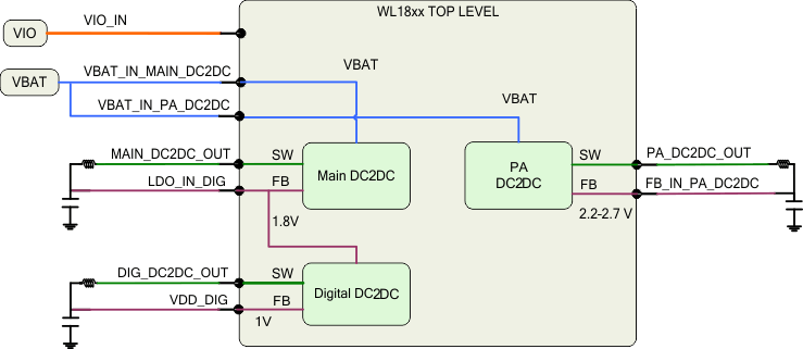 Figure 5-1 Internal DC2DCs
5.12.2 Power-Up and Shut-Down States
The correct power-up and shut-down sequences must be followed to avoid damage to the device.
While VBAT or VIO or both are deasserted, no signals should be driven to the device. The only exception is the slow clock that is a fail-safe I/O.
While VBAT, VIO, and slow clock are fed to the device, but WL_EN is deasserted (low), the device is in SHUTDOWN state. In SHUTDOWN state all functional blocks, internal DC2DCs, clocks, and LDOs are disabled.
To perform the correct power-up sequence, assert (high) WL_EN. The internal DC2DCs, LDOs, and clock start to ramp and stabilize. Stable slow clock, VIO, and VBAT are prerequisites to the assertion of one of the enable signals.
To perform the correct shut-down sequence, deassert (low) WL_EN while all the supplies to the device (VBAT, VIO, and slow clock) are still stable and available. The supplies to the chip (VBAT and VIO) can be deasserted only after both enable signals are deasserted (low).
Figure 5-2 shows the general power scheme for the module, including the powerdown sequence.

5.12.3 Chip Top-level Power-Up Sequence
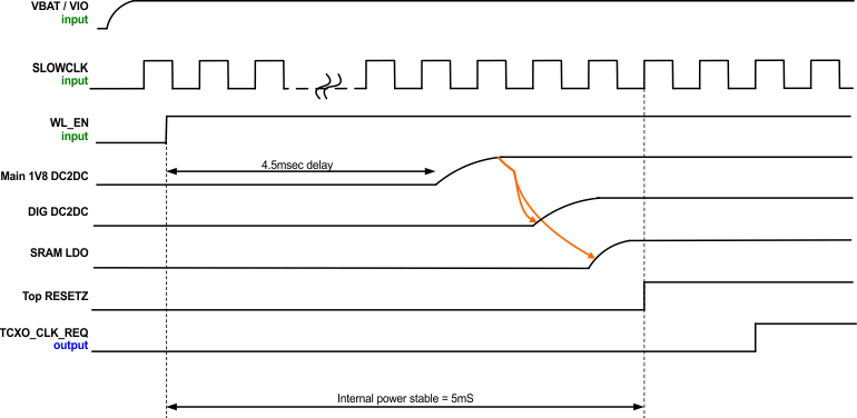 Figure 5-3 Chip Top-Level Power-Up Sequence
5.12.4 WLAN Power-Up Sequence
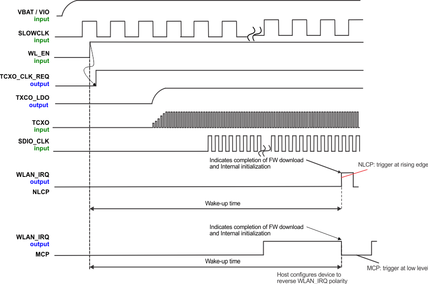 Figure 5-4 WLAN Power-Up Sequence
5.12.5 Bluetooth-BLE Power-Up Sequence
Figure 5-5 shows the Bluetooth-BLE power-up sequence.
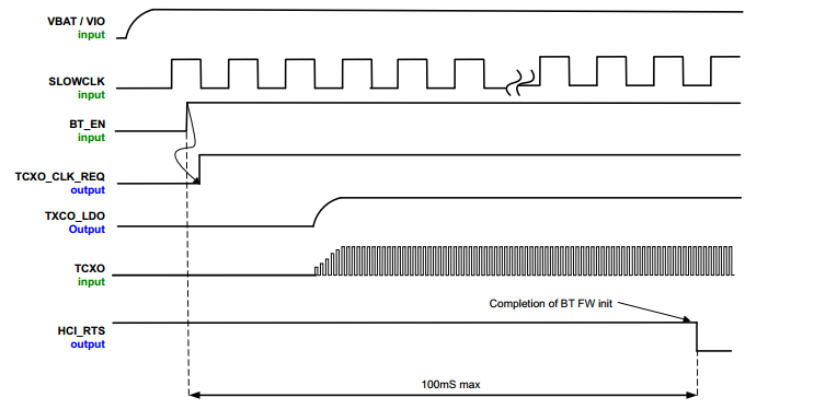 Figure 5-5 Bluetooth/BLE Power-Up Sequence
5.12.6 WLAN SDIO Transport Layer
The SDIO is the host interface for WLAN. The interface between the host and the WL18xx module uses an SDIO interface and supports a maximum clock rate of 50 MHz.
The device SDIO also supports the following features of the SDIO V3 specification:
- 4-bit data bus
- Synchronous and asynchronous in-band interrupt
- Default and high-speed (HS, 50 MHz) timing
- Sleep and wake commands
5.12.6.1 SDIO Timing Specifications
Figure 5-6 and Figure 5-7 show the SDIO switching characteristics over recommended operating conditions and with the default rate for input and output.
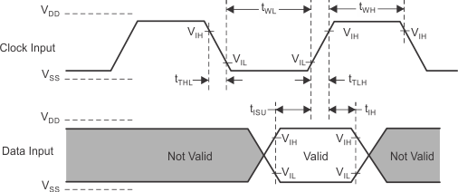 Figure 5-6 SDIO Default Input Timing
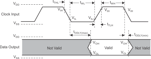 Figure 5-7 SDIO Default Output Timing
Table 5-1 lists the SDIO default timing characteristics.
Table 5-1 SDIO Default Timing Characteristics(1)
| PARAMETER(2) | MIN | MAX | UNIT | |
|---|---|---|---|---|
| fclock | Clock frequency, CLK | 0.0 | 26.0 | MHz |
| DC | Low, high duty cycle | 40.0 | 60.0 | % |
| tTLH | Rise time, CLK | 10.0 | ns | |
| tTHL | Fall time, CLK | 10.0 | ns | |
| tISU | Setup time, input valid before CLK ↑ | 3.0 | ns | |
| tIH | Hold time, input valid after CLK ↑ | 2.0 | ns | |
| tODLY | Delay time, CLK ↓ to output valid | 7.0 | 10.0 | ns |
| Cl | Capacitive load on outputs | 15.0 | pF | |
5.12.6.2 SDIO Switching Characteristics – High Rate
Figure 5-8 and Figure 5-9 show the parameters for maximum clock frequency.
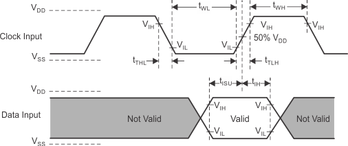 Figure 5-8 SDIO HS Input Timing
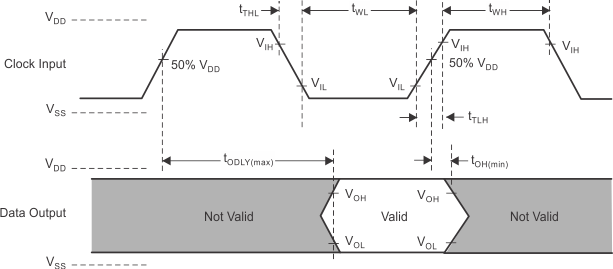 Figure 5-9 SDIO HS Output Timing
Table 5-2 lists the SDIO high-rate timing characteristics.
Table 5-2 SDIO HS Timing Characteristics
| PARAMETER | MIN | MAX | UNIT | |
|---|---|---|---|---|
| fclock | Clock frequency, CLK | 0.0 | 52.0 | MHz |
| DC | Low, high duty cycle | 40.0 | 60.0 | % |
| tTLH | Rise time, CLK | 3.0 | ns | |
| tTHL | Fall time, CLK | 3.0 | ns | |
| tISU | Setup time, input valid before CLK ↑ | 3.0 | ns | |
| tIH | Hold time, input valid after CLK ↑ | 2.0 | ns | |
| tODLY | Delay time, CLK ↑ to output valid | 7.0 | 10.0 | ns |
| Cl | Capacitive load on outputs | 10.0 | pF | |
5.12.7 HCI UART Shared Transport Layers for All Functional Blocks (Except WLAN)
The device incorporates a UART module dedicated to the Bluetooth shared-transport, host controller interface (HCI) transport layer. The HCI interface transports commands, events, and ACL between the Bluetooth device and its host using HCI data packets acting as a shared transport for all functional blocks except WLAN.
| WLAN | SHARED HCI FOR ALL FUNCTIONAL BLOCKS EXCEPT WLAN | BLUETOOTH VOICE-AUDIO |
|---|---|---|
| WLAN HS SDIO | Over UART | Bluetooth PCM |
The HCI UART supports most baud rates (including all PC rates) for all fast-clock frequencies up to a maximum of 4 Mbps. After power up, the baud rate is set for 115.2 kbps, regardless of the fast-clock frequency. The baud rate can then be changed using a VS command. The device responds with a Command Complete Event (still at 115.2 kbps), after which the baud rate change occurs.
HCI hardware includes the following features:
- Receiver detection of break, idle, framing, FIFO overflow, and parity error conditions
- Receiver-transmitter underflow detection
- CTS, RTS hardware flow control
- 4 wire (H4)
Table 5-3 lists the UART default settings.
Table 5-3 UART Default Setting
| PARAMETER | VALUE |
|---|---|
| Bit rate | 115.2 kbps |
| Data length | 8 bits |
| Stop bit | 1 |
| Parity | None |
5.12.7.1 UART 4-Wire Interface – H4
The interface includes four signals:
- TXD
- RXD
- CTS
- RTS
Flow control between the host and the device is byte-wise by hardware.
When the UART RX buffer of the device passes the flow-control threshold, the buffer sets the UART_RTS signal high to stop transmission from the host. When the UART_CTS signal is set high, the device stops transmitting on the interface. If HCI_CTS is set high in the middle of transmitting a byte, the device finishes transmitting the byte and stops the transmission.
Figure 5-10 shows the UART timing.
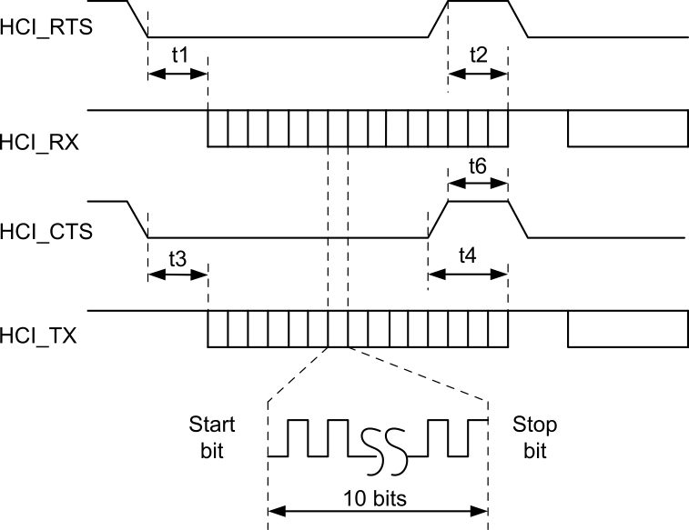 Figure 5-10 UART Timing Diagram
Table 5-4 lists the UART timing characteristics.
Table 5-4 UART Timing Characteristics
| PARAMETER | CONDITION | SYMBOL | MIN | TYP | MAX | UNIT |
|---|---|---|---|---|---|---|
| Baud rate | 37.5 | 4364 | Kbps | |||
| Baud rate accuracy per byte | Receive-transmit | –2.5 | +1.5 | % | ||
| Baud rate accuracy per bit | Receive-transmit | –12.5 | +12.5 | % | ||
| CTS low to TX_DATA on | t3 | 0.0 | 2.0 | µs | ||
| CTS high to TX_DATA off | Hardware flow control | t4 | 1.0 | Byte | ||
| CTS high pulse width | t6 | 1.0 | Bit | |||
| RTS low to RX_DATA on | t1 | 0.0 | 2.0 | µs | ||
| RTS high to RX_DATA off | Interrupt set to 1/4 FIFO | t2 | 16.0 | Bytes |
Figure 5-11 shows the UART data frame.
 Figure 5-11 UART Data Frame
5.12.8 Bluetooth Codec-PCM (Audio) Timing Specifications
Figure 5-12 shows the Bluetooth codec-PCM (audio) timing diagram.
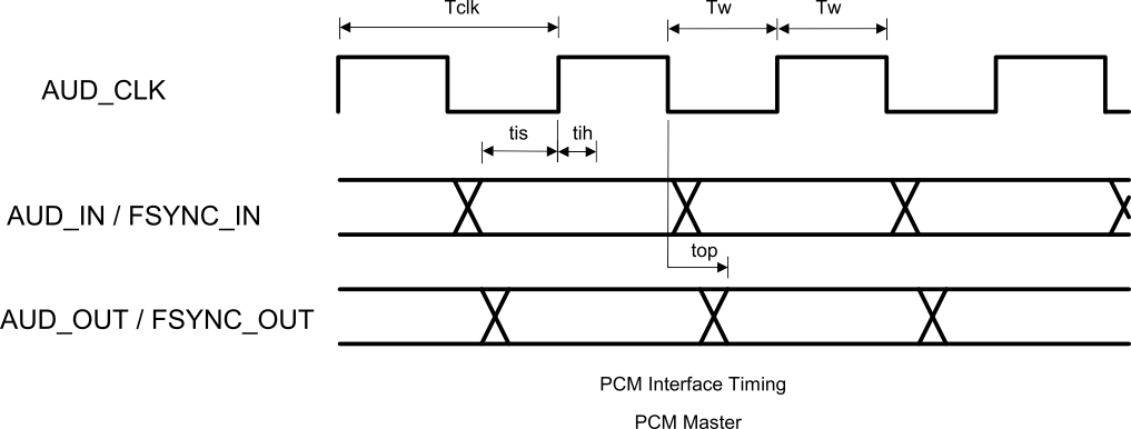 Figure 5-12 Bluetooth Codec-PCM (Audio) Master Timing Diagram
Table 5-5 lists the Bluetooth codec-PCM master timing characteristics.
Table 5-5 Bluetooth Codec-PCM Master Timing Characteristics
| PARAMETER | SYMBOL | MIN | MAX | UNIT |
|---|---|---|---|---|
| Cycle time | Tclk | 162.76 (6.144 MHz) | 15625 (64 kHz) | ns |
| High or low pulse width | Ts | 35% of Tclk min | ||
| AUD_IN setup time | tis | 10.6 | ||
| AUD_IN hold time | tih | 0 | ||
| AUD_OUT propagation time | top | 0 | 15 | |
| FSYNC_OUT propagation time | top | 0 | 15 | |
| Capacitive loading on outputs | Cl | 40 | pF |
Table 5-6 lists the Bluetooth codec-PCM slave timing characteristics.
Table 5-6 Bluetooth Codec-PCM Slave Timing Characteristics
| PARAMETER | SYMBOL | MIN | MAX | UNIT |
|---|---|---|---|---|
| Cycle time | Tclk | 81.38 (12.266 MHz) | ns | |
| High or low pulse width | Tw | 35% of Tclk min | ||
| AUD_IN setup time | tis | 5 | ||
| AUD_IN hold time | tih | 0 | ||
| AUD_FSYNC setup time | tis | 5 | ||
| AUD_FSYNC hold time | tih | 0 | ||
| AUD_OUT propagation time | top | 0 | 19 | |
| Capacitive loading on outputs | Cl | 40 | pF |