ZHCSC42J July 2013 – October 2014 WL1801MOD , WL1805MOD , WL1831MOD , WL1835MOD
PRODUCTION DATA.
- 1器件概述
- 2修订历史记录
- 3Device Comparison
- 4Terminal Configuration and Functions
-
5Specifications
- 5.1 Absolute Maximum Ratings
- 5.2 Handling Ratings
- 5.3 Power-On Hours (POH)
- 5.4 Recommended Operating Conditions
- 5.5 External Digital Slow Clock Requirements
- 5.6 Thermal Characteristics
- 5.7 WLAN Performance
- 5.8 Bluetooth Performance
- 5.9 Bluetooth LE Performance
- 5.10 Bluetooth-BLE Dynamic Currents
- 5.11 Bluetooth LE Currents
- 5.12
Timing and Switching Characteristics
- 5.12.1 Power Management
- 5.12.2 Power-Up and Shut-Down States
- 5.12.3 Chip Top-level Power-Up Sequence
- 5.12.4 WLAN Power-Up Sequence
- 5.12.5 Bluetooth-BLE Power-Up Sequence
- 5.12.6 WLAN SDIO Transport Layer
- 5.12.7 HCI UART Shared Transport Layers for All Functional Blocks (Except WLAN)
- 5.12.8 Bluetooth Codec-PCM (Audio) Timing Specifications
- 6Detailed Description
- 7Applications and Implementation
- 8Device and Documentation Support
- 9Mechanical Packaging and Orderable Information
6 Detailed Description
The WiLink 8 module is a self-contained connectivity solution based on WiLink 8 connectivity. As the eighth-generation connectivity combo chip from TI, the WiLink 8 module is based on proven technology.
Table 6-1 through Table 6-3 list performance parameters along with shutdown and sleep currents.
Table 6-1 WLAN Performance Parameters
| WLAN(3) | SPECIFICATION (TYP) | CONDITIONS |
|---|---|---|
| Maximum TX power | 17.3 dBm | 1 Mbps DSSS |
| Minimum sensitivity | –96.3 dBm | 1 Mbps DSSS |
| Sleep current | 160 µA | Leakage, firmware retained |
| Connected IDLE | 750 µA | No traffic IDLE connect |
| RX search | 54 mA | Search (SISO20) |
| RX current (SISO20) | 65 mA | MCS7, 2.4 GHz |
| TX current (SISO20)(1) | 238 mA | MCS7, 2.4 GHz, +11.2 dBm |
| Maximum peak current consumption during calibration(2) | 850 mA |
- At wakeup, the WiLink 8 module performs the entire calibration sequence at the center of the 2.4-GHz band.
- Once a link is established, calibration is performed periodically (every 5 minutes) on the specific channel tuned.
- The maximum VBAT value is based on peak calibration consumption with a 30% margin.
Table 6-2 Bluetooth Performance Parameters
| BLUETOOTH | SPECIFICATION (TYP) | CONDITIONS |
|---|---|---|
| Maximum TX power | 12.7 dBm | GFSK |
| Minimum sensitivity | –92.2 dBm | GFSK |
| Sniff | 178 µA | 1 attempt, 1.28 s (+4 dBm) |
| Page or inquiry | 253 µA | 1.28-s interrupt, 11.25-ms scan window (+4 dBm) |
| A2DP | 7.5 mA | MP3 high quality 192 kbps (+4 dBm) |
Table 6-3 Shutdown and Sleep Currents
| PARAMETER | POWER SUPPLY CURRENT | TYP | UNIT |
|---|---|---|---|
| Shutdown mode All functions shut down |
VBAT | 10 | µA |
| VIO | 2 | µA | |
| WLAN sleep mode | VBAT | 160 | µA |
| Bluetooth sleep mode | VBAT | 110 | µA |
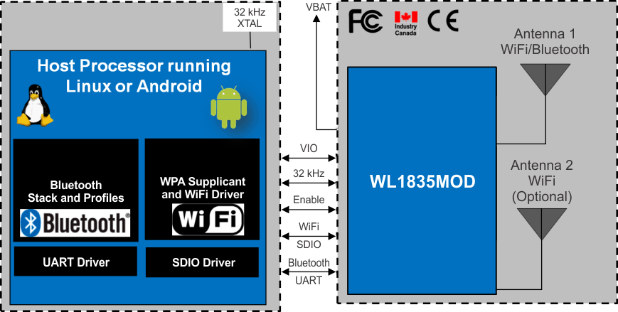
Figure 6-1 shows a high-level view of the WL1835MOD variant.
6.1 WLAN
The device supports the following WLAN features:
- Integrated 2.4-GHz power amplifiers (PAs) for a complete WLAN solution
- Baseband processor: IEEE Std 802.11b/g and IEEE Std 802.11n data rates with 20- or 40-MHz SISO and 20-MHz MIMO
- Fully calibrated system (production calibration not required)
- Medium access controller (MAC)
- Embedded ARM® central processing unit (CPU)
- Hardware-based encryption-decryption using 64-, 128-, and 256-bit WEP, TKIP, or AES keys
- Requirements for Wi-Fi-protected access (WPA and WPA2.0) and IEEE Std 802.11i (includes hardware-accelerated Advanced Encryption Standard [AES])
- New advanced coexistence scheme with Bluetooth and BLE
- 2.4-GHz radio
- Internal LNA and PA
- IEEE Std 802.11b, 802.11g, and 802.11n
- 4-bit SDIO host interface, including high speed (HS) and V3 modes
6.2 Bluetooth
The device supports the following Bluetooth features:
- Bluetooth 4.0 as well as CSA2
- Concurrent operation and built-in coexisting and prioritization handling of Bluetooth, BLE, audio processing, and WLAN
- Dedicated audio processor supporting on-chip SBC encoding + A2DP
- Assisted A2DP (A3DP): SBC encoding implemented internally
- Assisted WB-speech (AWBS): modified SBC codec implemented internally
6.3 BLE
The device supports the following BLE features:
- Bluetooth 4.0 BLE dual-mode standard
- All roles and role combinations, mandatory as well as optional
- Up to 10 BLE connections
- Independent LE buffering allowing many multiple connections with no affect on BR-EDR performance
6.4 WiLink 8 Module Markings
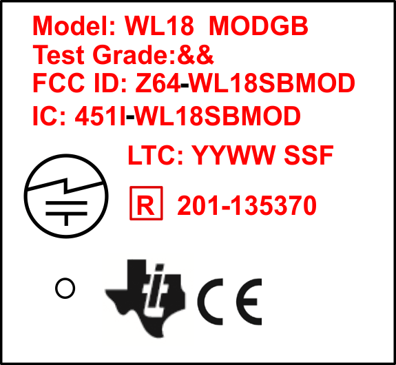
Figure 6-2 shows the markings for the TI WiLink 8 module.
 Figure 6-2 WiLink 8 Module Markings
Table 6-4 describes the WiLink 8 module markings.
Table 6-4 Description of WiLink 8 Module Markings
| MARKING | DESCRIPTION |
|---|---|
| WL18 MODGB | Model |
| && | Test grade (for more information, see Section 6.5, Test Grades) |
| Z64-WL18SBMOD | FCC ID: single modular FCC grant ID |
| 451I-WL18SBMOD | IC: single modular IC grant ID |
| YYWWSSF | LTC (lot trace code):
|
| 201-135370 | R: single modular TELEC grant ID |
 |
TELEC compliance mark |
| CE | CE compliance mark |
6.5 Test Grades
To minimize delivery time, TI may ship the device ordered or an equivalent device currently available that contains at least the functions of the part ordered. From all aspects, this device will behave exactly the same as the part ordered. For example, if a customer orders device WL1801MOD, the part shipped can be marked with a test grade of 37, 07 (see Table 6-5).
Table 6-5 Test Grade Markings
| MARK 1 | WLAN | BLUETOOTH |
|---|---|---|
| 0& | Tested | – |
| 3& | Tested | Tested |
| MARK 2 | WLAN 2.4 GHz | MIMO 2.4 GHz |
| &1 | Tested | – |
| &5 | Tested | Tested |
