ZHCSC42J July 2013 – October 2014 WL1801MOD , WL1805MOD , WL1831MOD , WL1835MOD
PRODUCTION DATA.
- 1器件概述
- 2修订历史记录
- 3Device Comparison
- 4Terminal Configuration and Functions
-
5Specifications
- 5.1 Absolute Maximum Ratings
- 5.2 Handling Ratings
- 5.3 Power-On Hours (POH)
- 5.4 Recommended Operating Conditions
- 5.5 External Digital Slow Clock Requirements
- 5.6 Thermal Characteristics
- 5.7 WLAN Performance
- 5.8 Bluetooth Performance
- 5.9 Bluetooth LE Performance
- 5.10 Bluetooth-BLE Dynamic Currents
- 5.11 Bluetooth LE Currents
- 5.12
Timing and Switching Characteristics
- 5.12.1 Power Management
- 5.12.2 Power-Up and Shut-Down States
- 5.12.3 Chip Top-level Power-Up Sequence
- 5.12.4 WLAN Power-Up Sequence
- 5.12.5 Bluetooth-BLE Power-Up Sequence
- 5.12.6 WLAN SDIO Transport Layer
- 5.12.7 HCI UART Shared Transport Layers for All Functional Blocks (Except WLAN)
- 5.12.8 Bluetooth Codec-PCM (Audio) Timing Specifications
- 6Detailed Description
- 7Applications and Implementation
- 8Device and Documentation Support
- 9Mechanical Packaging and Orderable Information
7 Applications and Implementation
7.1 Application Information
7.1.1 Typical Application – WL1835MOD Reference Design
Figure 7-1 shows the TI WL1835MOD reference design.
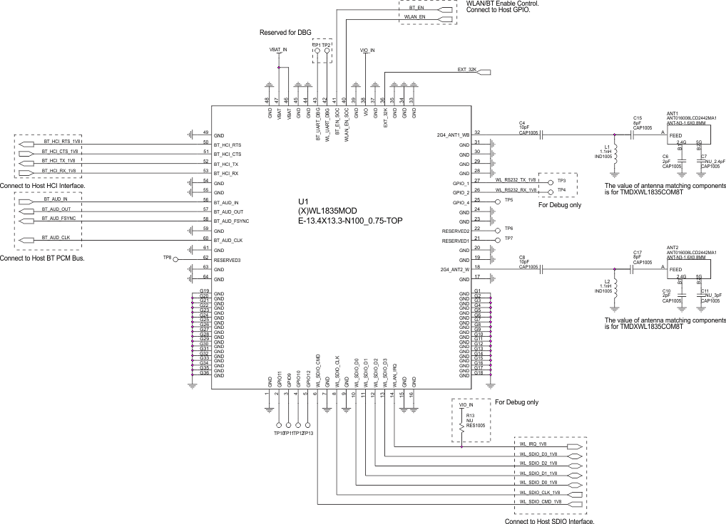 Figure 7-1 TI Module Reference Schematics
Table 7-1 lists the bill materials (BOM).
Table 7-1 Bill of Materials
| DESCRIPTION | PART NUMBER | PACKAGE | REFERENCE | QTY | MFR |
|---|---|---|---|---|---|
| TI WL 1835 WiFi/BT Module | (X)WL1835MOD | 13.4 x 13.3 x 2.0mm | U1 | 1 | TI |
| ANT/Chip/2.4, 5 GHz/Peak Gain > 5 dBi | ANT016008LCD2442MA1 | 1.6 mm x 0.8 mm | ANT1, ANT2 | 2 | TDK |
| IND 0402/1.2 nH/±0.3/0.12 Ω/300 mA | Hl1005-1C1N2SMT | 0402 | L1, L2 | 2 | ACX |
| CAP 0402/2.0 pF/50 V/C0G/±0.25 pF | C1005C0G1H020C | 0402 | C8, C10 | 2 | Walsin |
| CAP 0402/8.2 pF/50 V/NPO/±0.5 pF | 0402N8R2D500 | 0402 | C15, C17 | 2 | Walsin |
| CAP 0402/10 pF/50 V/NPO/±5% | 0402N100J500LT | 0402 | C4, C6 | 2 | Walsin |
| RES 0402/10K/±5% (debug only) | WR04X103 JTL | 0402 | R13 | 1 | Walsin |
7.1.2 Design Recommendations
This section describes the layout recommendations for the (X)WL1835 module, RF trace, and antenna.
Table 7-2 summarizes the layout recommendations.
Table 7-2 Layout Recommendations Summary
| ITEM | DESCRIPTION |
|---|---|
| Thermal | |
| 1 | The proximity of ground vias must be close to the pad. |
| 2 | Signal traces must not be run underneath the module on the layer where the module is mounted. |
| 3 | Have a complete ground pour in layer 2 for thermal dissipation. |
| 4 | Have a solid ground plane and ground vias under the module for stable system and thermal dissipation. |
| 5 | Increase the ground pour in the first layer and have all of the traces from the first layer on the inner layers, if possible. |
| 6 | Signal traces can be run on a third layer under the solid ground layer, which is below the module mounting layer. |
| RF Trace and Antenna Routing | |
| 7 | The RF trace antenna feed must be as short as possible beyond the ground reference. At this point, the trace starts to radiate. |
| 8 | The RF trace bends must be gradual with an approximate maximum bend of 45 degrees with trace mitered. RF traces must not have sharp corners. |
| 9 | RF traces must have via stitching on the ground plane beside the RF trace on both sides. |
| 10 | RF traces must have constant impedance (microstrip transmission line). |
| 11 | For best results, the RF trace ground layer must be the ground layer immediately below the RF trace. The ground layer must be solid. |
| 12 | There must be no traces or ground under the antenna section. |
| 13 | RF traces must be as short as possible. The antenna, RF traces, and modules must be on the edge of the PCB product. The proximity of the antenna to the enclosure and the enclosure material must also be considered. |
| Supply and IF | |
| 14 | The power trace for VBAT must be at least 40-mil wide. |
| 15 | The 1.8-V trace must be at least 18-mil wide. |
| 16 | Make VBAT traces as wide as possible to ensure reduced inductance and trace resistance. |
| 17 | If possible, shield VBAT traces with ground above, below, and beside the traces. |
| 18 | SDIO signals traces (CLK, CMD, D0, D1, D2, and D3) must be routed in parallel to each other and as short as possible (less than 12 cm). In addition, every trace length must be the same as the others. There should be enough space between traces – greater than 1.5 times the trace width or ground – to ensure signal quality, especially for the SDIO_CLK trace. Remember to keep these traces away from the other digital or analog signal traces. TI recommends adding ground shielding around these buses. |
| 19 | SDIO and digital clock signals are a source of noise. Keep the traces of these signals as short as possible. If possible, maintain a clearance around them. |
7.1.3 RF Trace and Antenna Layout Recommendations
Figure 7-2 shows the location of the antenna on the WL1835MODCOM8 board as well as the RF trace routing from the (X)WL1835 module (TI reference design). The TDK chip multilayer antennas are mounted on the board with a specific layout and matching circuit for the radiation test conducted in FCC, CE, and IC certifications.
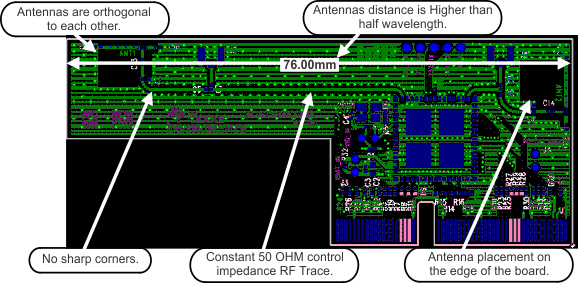 Figure 7-2 Location of Antenna and RF Trace Routing on the TMDXWL1835MODCOM8T Board
Follow these RF trace routing recommendations:
- RF traces must have 50-Ω impedance.
- RF traces must not have sharp corners.
- RF traces must have via stitching on the ground plane beside the RF trace on both sides.
- RF traces must be as short as possible. The antenna, RF traces, and module must be on the edge of the PCB product in consideration of the product enclosure material and proximity.
7.1.4 Module Layout Recommendations
Figure 7-3 shows layer 1 and layer 2 of the TI module layout:
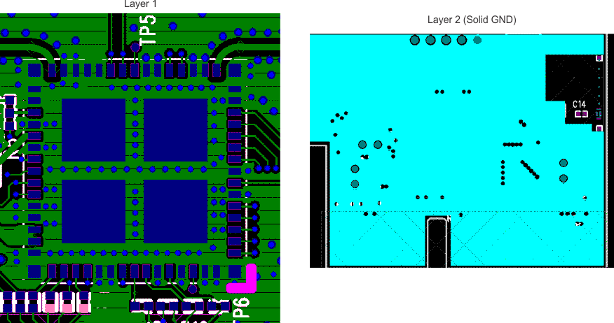 Figure 7-3 TI Module Layout
Follow these module layout recommendations:
- Ensure a solid ground plane and ground vias under the module for stable system and thermal dissipation.
- Do not run signal traces underneath the module on a layer where the module is mounted.
- Signal traces can be run on a third layer under the solid ground layer and beneath the module mounting.
- Run the host interfaces with ground on the adjacent layer to improve the return path.
- TI recommends routing the signals as short as possible to the host.
7.1.5 Thermal Board Recommendations
The TI module uses µvias for layers 1 through 6 with full copper filling, providing heat flow all the way to the module ground pads.
TI recommends using one big ground pad under the module with vias all the way to connect the pad to all ground layers (see Figure 7-4).
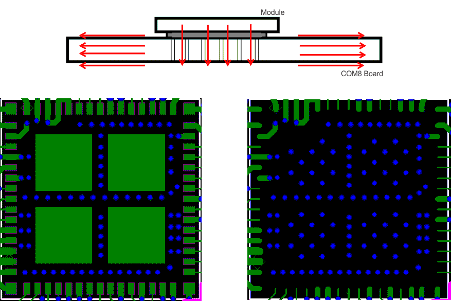 Figure 7-4 Block of Ground Pads on Bottom Side of Package
Figure 7-5 shows via array patterns, which are applied wherever possible to connect all of the layers to the TI module central or main ground pads.
 Figure 7-5 Via Array Patterns
7.1.6 Baking and SMT Recommendations
7.1.6.1 Baking Recommendations
Follow these baking guidelines for the WiLink 8 module:
- Follow MSL level 3 to perform the baking process.
- After the bag is open, devices subjected to reflow solder or other high temperature processes must be mounted within 168 hours of factory conditions (< 30°C/60% RH) or stored at <10% RH.
- if the Humidity Indicator Card reads >10%, devices require baking before being mounted.
- If baking is required, bake devices for 8 hours at 125 °C.
7.1.6.2 SMT Recommendations
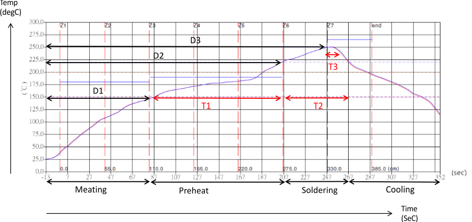
Figure 7-6 shows the recommended reflow profile for the WiLink 8 module.
Table 7-3 lists the temperature values for the profile shown in Figure 7-6.
