ZHCSC42J July 2013 – October 2014 WL1801MOD , WL1805MOD , WL1831MOD , WL1835MOD
PRODUCTION DATA.
- 1器件概述
- 2修订历史记录
- 3Device Comparison
- 4Terminal Configuration and Functions
-
5Specifications
- 5.1 Absolute Maximum Ratings
- 5.2 Handling Ratings
- 5.3 Power-On Hours (POH)
- 5.4 Recommended Operating Conditions
- 5.5 External Digital Slow Clock Requirements
- 5.6 Thermal Characteristics
- 5.7 WLAN Performance
- 5.8 Bluetooth Performance
- 5.9 Bluetooth LE Performance
- 5.10 Bluetooth-BLE Dynamic Currents
- 5.11 Bluetooth LE Currents
- 5.12
Timing and Switching Characteristics
- 5.12.1 Power Management
- 5.12.2 Power-Up and Shut-Down States
- 5.12.3 Chip Top-level Power-Up Sequence
- 5.12.4 WLAN Power-Up Sequence
- 5.12.5 Bluetooth-BLE Power-Up Sequence
- 5.12.6 WLAN SDIO Transport Layer
- 5.12.7 HCI UART Shared Transport Layers for All Functional Blocks (Except WLAN)
- 5.12.8 Bluetooth Codec-PCM (Audio) Timing Specifications
- 6Detailed Description
- 7Applications and Implementation
- 8Device and Documentation Support
- 9Mechanical Packaging and Orderable Information
9 Mechanical Packaging and Orderable Information
9.1 TI Module Mechanical Outline
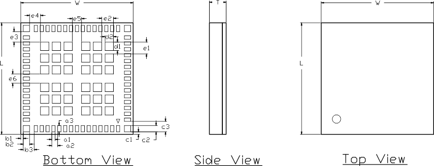
Figure 9-1 shows the mechanical outline for the device.
 Figure 9-1 TI Module Mechanical Outline
Table 9-1 lists the dimensions for the mechanical outline of the device.
Table 9-1 Dimensions for TI Module Mechanical Outline
| MARKING | MIN (mm) | NOM (mm) | MAX (mm) | MARKING | MIN (mm) | NOM (mm) | MAX (mm) | |
|---|---|---|---|---|---|---|---|---|
| L (body size) | 13.20 | 13.30 | 13.40 | c2 | 0.65 | 0.75 | 0.85 | |
| W (body size) | 13.30 | 13.40 | 13.50 | c3 | 1.15 | 1.25 | 1.35 | |
| T (thickness) | 1.90 | 2.00 | d1 | 0.90 | 1.00 | 1.10 | ||
| a1 | 0.30 | 0.40 | 0.50 | d2 | 0.90 | 1.00 | 1.10 | |
| a2 | 0.60 | 0.70 | 0.80 | e1 | 1.30 | 1.40 | 1.50 | |
| a3 | 0.65 | 0.75 | 0.85 | e2 | 1.30 | 1.40 | 1.50 | |
| b1 | 0.20 | 0.30 | 0.40 | e3 | 1.15 | 1.25 | 1.35 | |
| b2 | 0.65 | 0.75 | 0.85 | e4 | 1.20 | 1.30 | 1.40 | |
| b3 | 1.20 | 1.30 | 1.40 | e5 | 1.00 | 1.10 | 1.20 | |
| c1 | 0.20 | 0.30 | 0.40 | e6 | 1.00 | 1.10 | 1.20 |
9.2 Packaging Information
The following pages include mechanical packaging and orderable information. This information is the most current data available for the designated devices. This data is subject to change without notice and revision of this document. For browser-based versions of this data sheet, refer to the left-hand navigation.