ZHCSHO6 February 2018 XTR305
PRODUCTION DATA.
- 1 特性
- 2 应用
- 3 说明
- 4 修订历史记录
- 5 Pin Configuration and Functions
-
6 Specifications
- 6.1 Absolute Maximum Ratings
- 6.2 ESD Ratings
- 6.3 Recommended Operating Conditions
- 6.4 Thermal Information
- 6.5 Electrical Characteristics: Voltage Output Mode
- 6.6 Electrical Characteristics: Current Output Mode
- 6.7 Electrical Characteristics: Operational Amplifier (OPA)
- 6.8 Electrical Characteristics: Instrumentation Amplifier (IA)
- 6.9 Electrical Characteristics: Current Monitor
- 6.10 Electrical Characteristics: Power and Digital
- 6.11 Typical Characteristics
- 7 Detailed Description
-
8 Application and Implementation
- 8.1 Application Information
- 8.2
Typical Application
- 8.2.1 Design Requirements
- 8.2.2
Detailed Design Procedure
- 8.2.2.1 Voltage Output Mode
- 8.2.2.2 Current Output Mode
- 8.2.2.3 Input Signal Connection
- 8.2.2.4 Externally-Configured Mode: OPA and IA
- 8.2.2.5 Driver Output Disable
- 8.2.2.6 Driving Capacitive Loads and Loop Compensation
- 8.2.2.7 Internal Current Sources, Switching Noise, and Settling Time
- 8.2.2.8 IA Structure, Voltage Monitor
- 8.2.2.9 Digital I/O and Ground Considerations
- 8.2.2.10 Output Protection
- 8.2.3 Application Curves
- 9 Power Supply Recommendations
- 10Layout
- 11器件和文档支持
- 12机械、封装和可订购信息
7.3.4 Power On/Off Glitch
When power is turned on or off, most analog amplifiers generate some glitching of the output because of internal circuit thresholds and capacitive charges. Characteristics of the supply voltage, as well as its rise and fall time, directly influence output glitches. Load resistance and capacitive load also affect the amplitude.
The output disable control (OD) cannot fully suppress glitches during power-on and power-off, but reduces the energy significantly. The glitch consists of a small amount of current and capacitive charge (voltage) that reacts with the resistive and capacitive load. The bias current of the IA inputs that are normally connected to the output also generate a voltage across the load.
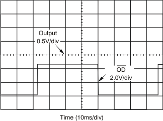
Figure 38 indicates no glitches when transitioning between disable and enable. This measurement is made with a load resistance of 1 kΩ and tested in the circuit configuration of Figure 40.
 Figure 38. Output Signal During Toggle of OD
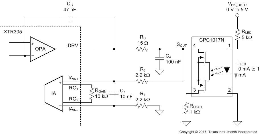
When the power is off or with low supply, the output is diode clamped to the momentary supply voltage, but can float while output disabled within those limits unless terminated. Only an external switch (relays or opto-relays) can isolate the output under such conditions. Refer to Figure 39 for an illustration of this configuration. The same consideration applies if low impedance zero output is required, even during power off.
 Figure 39. Example for Opto-Relay Output Isolation