ZHCSHO6 February 2018 XTR305
PRODUCTION DATA.
- 1 特性
- 2 应用
- 3 说明
- 4 修订历史记录
- 5 Pin Configuration and Functions
-
6 Specifications
- 6.1 Absolute Maximum Ratings
- 6.2 ESD Ratings
- 6.3 Recommended Operating Conditions
- 6.4 Thermal Information
- 6.5 Electrical Characteristics: Voltage Output Mode
- 6.6 Electrical Characteristics: Current Output Mode
- 6.7 Electrical Characteristics: Operational Amplifier (OPA)
- 6.8 Electrical Characteristics: Instrumentation Amplifier (IA)
- 6.9 Electrical Characteristics: Current Monitor
- 6.10 Electrical Characteristics: Power and Digital
- 6.11 Typical Characteristics
- 7 Detailed Description
-
8 Application and Implementation
- 8.1 Application Information
- 8.2
Typical Application
- 8.2.1 Design Requirements
- 8.2.2
Detailed Design Procedure
- 8.2.2.1 Voltage Output Mode
- 8.2.2.2 Current Output Mode
- 8.2.2.3 Input Signal Connection
- 8.2.2.4 Externally-Configured Mode: OPA and IA
- 8.2.2.5 Driver Output Disable
- 8.2.2.6 Driving Capacitive Loads and Loop Compensation
- 8.2.2.7 Internal Current Sources, Switching Noise, and Settling Time
- 8.2.2.8 IA Structure, Voltage Monitor
- 8.2.2.9 Digital I/O and Ground Considerations
- 8.2.2.10 Output Protection
- 8.2.3 Application Curves
- 9 Power Supply Recommendations
- 10Layout
- 11器件和文档支持
- 12机械、封装和可订购信息
8.2.2.2 Current Output Mode
The XTR305 does not require a shunt resistor for current control because it uses a precise current mirror arrangement.
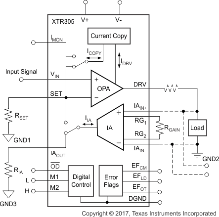
In current output mode (M1 connected low, or left unconnected and M2 connected high), a precise copy of 1/10th of the output is internally routed back to the summing junction of the OPA through a multiplexer, closing the control loop for the output current.
The OPA driver can deliver more than ±24 mA within a wide output voltage range. An open-output condition or high-impedance load that prevents the flow of the required current activates the EFLD flag and the IA can become overloaded and draw greater than 7-mA saturation current.
While in current output mode, a current (IIA) that is proportional to the voltage at the IA input is routed to IAOUT and can be used to monitor the load voltage. A resistor converts this current into voltage. This arrangement makes level shifting easy.
Alternatively, the IA can be used as an independent monitoring channel. If this output is not used, connect it to GND to maintain proper function of the monitor stage, as shown in Figure 42.
 Figure 42. Simplified Current Output Mode Configuration
The transconductance (gain) can be set by the resistor, RSET, according to Equation 3:

or when adding an offset VREF to get bidirectional output with a single-ended input shown in Equation 4:
