ZHCSHO6 February 2018 XTR305
PRODUCTION DATA.
- 1 特性
- 2 应用
- 3 说明
- 4 修订历史记录
- 5 Pin Configuration and Functions
-
6 Specifications
- 6.1 Absolute Maximum Ratings
- 6.2 ESD Ratings
- 6.3 Recommended Operating Conditions
- 6.4 Thermal Information
- 6.5 Electrical Characteristics: Voltage Output Mode
- 6.6 Electrical Characteristics: Current Output Mode
- 6.7 Electrical Characteristics: Operational Amplifier (OPA)
- 6.8 Electrical Characteristics: Instrumentation Amplifier (IA)
- 6.9 Electrical Characteristics: Current Monitor
- 6.10 Electrical Characteristics: Power and Digital
- 6.11 Typical Characteristics
- 7 Detailed Description
-
8 Application and Implementation
- 8.1 Application Information
- 8.2
Typical Application
- 8.2.1 Design Requirements
- 8.2.2
Detailed Design Procedure
- 8.2.2.1 Voltage Output Mode
- 8.2.2.2 Current Output Mode
- 8.2.2.3 Input Signal Connection
- 8.2.2.4 Externally-Configured Mode: OPA and IA
- 8.2.2.5 Driver Output Disable
- 8.2.2.6 Driving Capacitive Loads and Loop Compensation
- 8.2.2.7 Internal Current Sources, Switching Noise, and Settling Time
- 8.2.2.8 IA Structure, Voltage Monitor
- 8.2.2.9 Digital I/O and Ground Considerations
- 8.2.2.10 Output Protection
- 8.2.3 Application Curves
- 9 Power Supply Recommendations
- 10Layout
- 11器件和文档支持
- 12机械、封装和可订购信息
8.2.2.3 Input Signal Connection
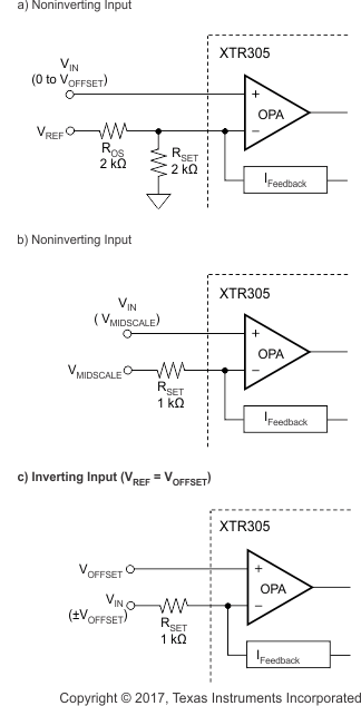
It is possible to drive the XTR305 with a unidirectional input signal and still get a bidirectional output by adding an additional resistor, ROS, and an offset voltage signal, VREF. It can be a mid-point voltage or a signal to shift the output voltage to a desired value.
This design is illustrated in Figure 43a, Figure 43b, and Figure 43c. As with a normal operational amplifier, there are several options for offset-shift circuits. The input can be connected for inverting or noninverting gain. Unlike many op amp input circuits, however, this configuration uses current feedback, which removes the voltage relationship between the noninverting input and output potential because there is no feedback resistor.
 Figure 43. Circuit Options for Op Amp Output Level Shifting
The input bias current effect on the offset voltage can be reduced by connecting a resistor in series with the positive input that matches the approximate resistance at the negative input. This resistor placed close to the input pin acts as a damping element and makes the design less sensitive to RF noise. See R3 in Figure 40.