ZHCSHO6 February 2018 XTR305
PRODUCTION DATA.
- 1 特性
- 2 应用
- 3 说明
- 4 修订历史记录
- 5 Pin Configuration and Functions
-
6 Specifications
- 6.1 Absolute Maximum Ratings
- 6.2 ESD Ratings
- 6.3 Recommended Operating Conditions
- 6.4 Thermal Information
- 6.5 Electrical Characteristics: Voltage Output Mode
- 6.6 Electrical Characteristics: Current Output Mode
- 6.7 Electrical Characteristics: Operational Amplifier (OPA)
- 6.8 Electrical Characteristics: Instrumentation Amplifier (IA)
- 6.9 Electrical Characteristics: Current Monitor
- 6.10 Electrical Characteristics: Power and Digital
- 6.11 Typical Characteristics
- 7 Detailed Description
-
8 Application and Implementation
- 8.1 Application Information
- 8.2
Typical Application
- 8.2.1 Design Requirements
- 8.2.2
Detailed Design Procedure
- 8.2.2.1 Voltage Output Mode
- 8.2.2.2 Current Output Mode
- 8.2.2.3 Input Signal Connection
- 8.2.2.4 Externally-Configured Mode: OPA and IA
- 8.2.2.5 Driver Output Disable
- 8.2.2.6 Driving Capacitive Loads and Loop Compensation
- 8.2.2.7 Internal Current Sources, Switching Noise, and Settling Time
- 8.2.2.8 IA Structure, Voltage Monitor
- 8.2.2.9 Digital I/O and Ground Considerations
- 8.2.2.10 Output Protection
- 8.2.3 Application Curves
- 9 Power Supply Recommendations
- 10Layout
- 11器件和文档支持
- 12机械、封装和可订购信息
10.1 Layout Guidelines
Supply bypass capacitors must be close to the package and connected with low-impedance conductors. Avoid noise coupled into RGAIN, and observe wiring resistance. For thermal management, see the VQFN Package and Heat Sinking section.
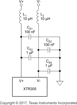
Layout for the XTR305 is not critical; however, its internal current chopping works best with good (low dynamic impedance) supply decoupling. Therefore, avoid through-hole contacts in the connection to the bypass capacitors or use multiple through-hole contacts. Switching noise from power supplies should be filtered enough to reduce influence on the circuit. Small resistors (2-Ω, for example) or damping inductors in series with the supply connection (between the DC-DC converter and the XTR circuit) act as a decoupling filter together with the bypass capacitor as shown in Figure 49.
Resistors connected close to the input pins help dampen environmental noise coupled into conductor traces. Therefore, place the OPA input- and IA input-related resistors close to the package. Also, avoid additional wire resistance in series to RSET, ROS, and RGAIN (observe the reliability of the through-hole contacts), because this resistance could produce gain and offset error as well as drift; 1 Ω is already 0.1% of the 1-kΩ resistor.
The exposed lead-frame die pad on the bottom of the package must be connected to V−, pin 11 (see the VQFN Package and Heat Sinking section for more details).
 Figure 49. Suggested Supply Decoupling for Noisy Chopper-Type Supplies