SBAA461 December 2020 ADC3541 , ADC3542 , ADC3543 , ADC3544 , ADC3641 , ADC3642 , ADC3643 , ADC3644 , ADC3660 , ADC3681 , ADC3682 , ADC3683
1 Introduction
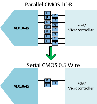
High Speed SAR ADCs incorporate precision features (for example, excellent DC linearity and AC performance) while also allowing for sampling rates above 10 MSPS at ultra-low power consumption. With higher sampling speeds comes higher output data rates, so FPGA's are typically used to handle these higher speed CMOS and LVDS interfaces. However, there are trade-offs that can be made to reduce data rates and pin count while maintaining (or improving) the performance your application demands which can open the door for lower cost ADC data capture solutions (micro controllers and low cost FPGAs).
 Figure 1-1 ADC3643 2CH CMOS
Interfaces