SBAA461 December 2020 ADC3541 , ADC3542 , ADC3543 , ADC3544 , ADC3641 , ADC3642 , ADC3643 , ADC3644 , ADC3660 , ADC3681 , ADC3682 , ADC3683
2.2.1 2 Wire
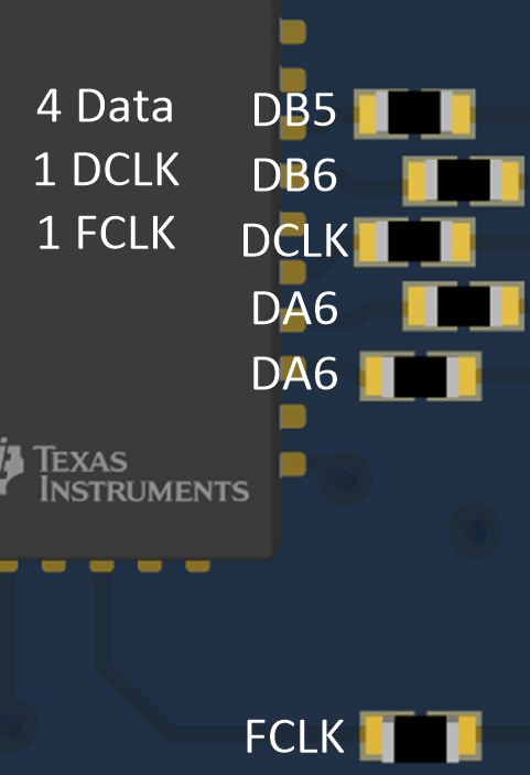
In 2 Wire mode, all 14 bits of one channel are being transmitted on two wires, 7 bits per wire. In a 2CH ADC (ADC3643), there are a total of 6 data outputs/resistors: 4 data resistors (2 per channel), 1 Data Clock and 1 Frame Clock.
 Figure 2-5 ADC3643 Serial CMOS: 2 Wire
Resistors
Figure 2-5 ADC3643 Serial CMOS: 2 Wire
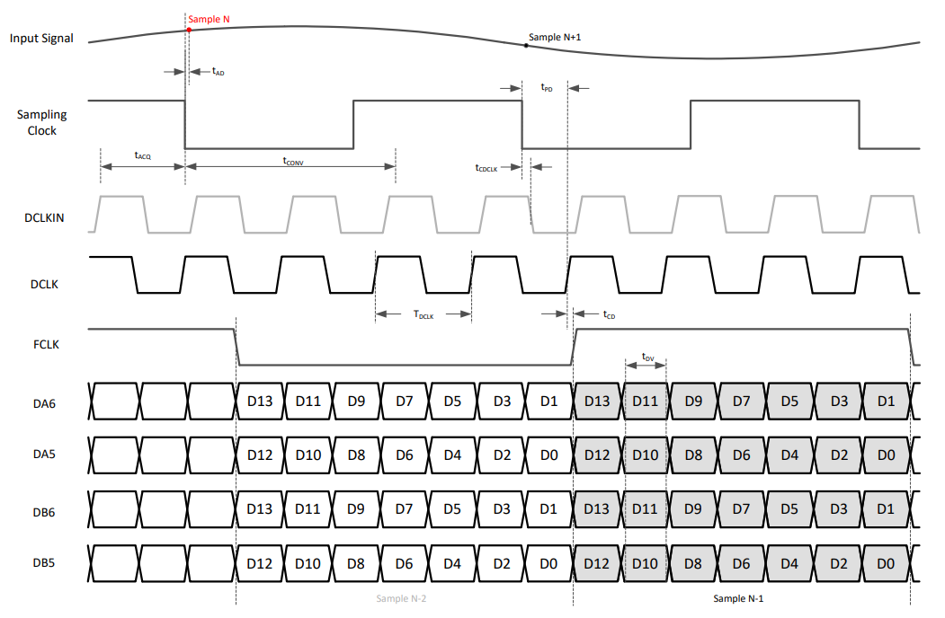
ResistorsA total of 7 bits per wire will be transmitted over one frame clock period. The serialization rate is 7x times the sampling rate. The data rate is limited to ~250 due to the CMOS interface, so the max sampling rate in this mode is 35 MSPS. Higher sampling rates can be used when decimation is used.
|
Mode |
Max Sampling Rate (MSPS) |
Serialization Rate |
Data Rate (Mbps) |
Data Outputs/ Resistors |
|---|---|---|---|---|
|
2 Wire |
35 |
7 |
250 |
6 |
 Figure 2-6 Serial CMOS 2W Timing
Diagram