SBAA531 November 2021 ADS8860 , ADS8862 , ADS8881 , ADS9110 , ADS9224R
- Trademarks
- 1Introduction
-
2
Internal Topology of SAR ADC Model
- 2.1 Sample and Hold
- 2.2 Sample and Hold Timing
- 2.3 Reference Transients
- 2.4 Bandwidth Modeling
- 2.5 Noise Modeling
- 2.6 Reference Droop and Reference Noise Errors
- 2.7 Gain, Offset, and Input Leakage Modeling
- 2.8 Differential input behavior
- 2.9 ESD Protection Diodes and Parasitic Capacitance
- 2.10 Summary of Parameters
- 2.11 Summary of Model Pins
- 3Downloading and Using PSpice® Example Projects From Web
- 4Summary
2.4 Bandwidth Modeling
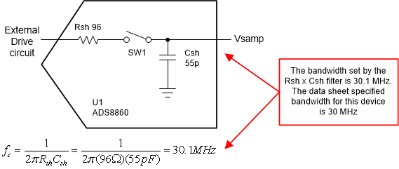
The bandwidth of the input circuit depends mainly on the sample and hold circuit. The input resistor Rsh and input capacitor Csh can be used to calculate the bandwidth. Some SAR ADC data sheets show a specified bandwidth that is slightly different from the bandwidth set by the input Rsh × Csh filter, but typically this difference is very small and can be neglected. The bandwidth of the ADC is very important in noise simulations as proper bandwidth modeling allows calculation of total noise. Figure 2-5 illustrates how the internal bandwidth is set by the sample and hold circuit.
 Figure 2-5 Bandwidth of ADC