SBAA531 November 2021 ADS8860 , ADS8862 , ADS8881 , ADS9110 , ADS9224R
- Trademarks
- 1Introduction
-
2
Internal Topology of SAR ADC Model
- 2.1 Sample and Hold
- 2.2 Sample and Hold Timing
- 2.3 Reference Transients
- 2.4 Bandwidth Modeling
- 2.5 Noise Modeling
- 2.6 Reference Droop and Reference Noise Errors
- 2.7 Gain, Offset, and Input Leakage Modeling
- 2.8 Differential input behavior
- 2.9 ESD Protection Diodes and Parasitic Capacitance
- 2.10 Summary of Parameters
- 2.11 Summary of Model Pins
- 3Downloading and Using PSpice® Example Projects From Web
- 4Summary
2.2 Sample and Hold Timing
As previously mentioned, the conversion cycle is broken into an acquisition phase where the sample and hold switch is closed and a conversion phase where the switch is opened and the sampled signal is held. The conversion period is a fixed amount of time set by an internal oscillator or external clock signal. Most converters transition to the acquisition period whenever the ADC is not converting. For example, assume the converter has a conversion phase (TCONV) that lasts for 710 ns. If the device sampling rate is 1 Msps, or 1 sample/µs, then the acquisition period can be calculated by subtracting the conversion phase from the device throughput (tacq = throughput – TCONV= 1 µs – 710 ns = 290 ns). Furthermore, if the sampling rate is reduced to 100 ksps, the conversion period remains the same and the acquisition period naturally gets longer (tacq = 10 µs – 710 ns = 9.29 µs ).
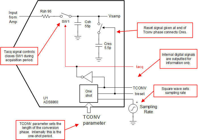
The model includes a parameter to set TCONV, and uses an external square wave to set the sampling rate. The external square wave triggers an internal one-shot timer that initiates the conversion phase. The conversion phase lasts for a time specified by the parameter TCONV. Inside the model the parameter TCONVis used to set the timing capacitor for the one-shot. Whenever the device is not converting it is acquiring, so the tacq signal is the inversion of TCONV.
The TCONVand tacq signals are used to control the timing of the sample and hold circuit. The sample and hold switch is closed throughout the tacq period and open during the TCONV period. At the end of the TCONVperiod a small reset sample and hold signal is generated. This signal connects Csh in parallel with a reset capacitor. The reset capacitor initially charged to 0 V, so when it is connected in parallel with Csh it causes the voltage on Csh to droop. This droop emulates the real-world behavior of a sample and hold circuit. The droop happens as a result of the conversion process and typically it is about 10% of the held voltage. Thus, Creset is typically sized to be 10% of Csh. Figure 2-2 below shows the sample and hold timing control.
 Figure 2-2 Sample and Hold Timing Control