SBAA551 June 2022 ADS8661 , ADS8665 , ADS8671 , ADS8675 , ADS8681 , ADS8685 , ADS8689 , ADS8691 , ADS8695 , ADS8699 , INA823 , INA826 , LM317L , LM337L , MUX509 , TPS2661 , TPS560430
3.4 Settling Time
Settling time specifies the time it takes to switch from one input channel (here: ch1) to another input channel (here: ch2) and the newly selected channel has settled across the analog front-end. The settling time is dictated mainly by the 2nd-order LPF inside the ADC. The preceding front-end should be fast enough not to influence the LPF settling time. This is achieved when a settled signal for each channel is available at the MUX input and settling after the MUX is reduced to a minimum.
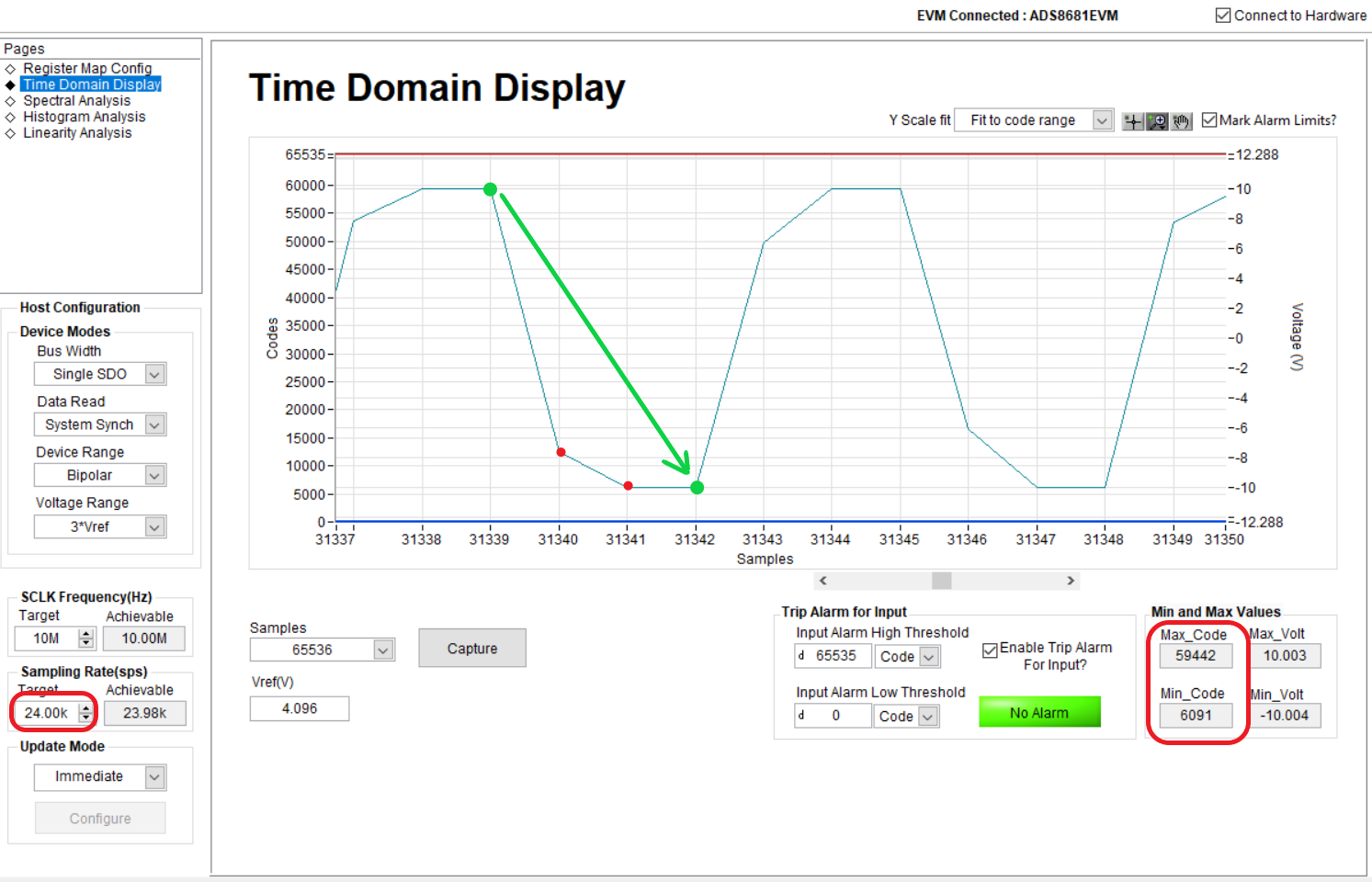
Worst case, the input signal of the last channel is the opposite of the new channel, here VIN_DIFF_CH1 = –10 V and VIN_DIFF_CH2 = 10 V. Both channels are continuously and alternating converted. Only if both channels reach their steady state values (compare table 3 for steady state values for –10-V and +10-V input signals) the settling is considered complete. Due to demonstration software limitations, a sampling frequency of 24 kSPS (instead of 8 kSPS) was selected. Consequently, the 3rd conversion after each new channel selection is valid. The following image shows the proper settling within 115 μs (125μs (equals 8 kSPS) -10 μs (conversion time)) as the steady-state code for each channel (table 3) matches the codes in the lower-right corner.
 Figure 3-2 Settling Time Verification