SBAS108E May 2000 – December 2016 ADS8320
PRODUCTION DATA.
- 1 Features
- 2 Applications
- 3 Description
- 4 Revision History
- 5 Pin Configuration and Functions
- 6 Specifications
- 7 Detailed Description
- 8 Application and Implementation
- 9 Power Supply Recommendations
- 10Layout
- 11Device and Documentation Support
- 12Mechanical, Packaging, and Orderable Information
8 Application and Implementation
NOTE
Information in the following applications sections is not part of the TI component specification, and TI does not warrant its accuracy or completeness. TI’s customers are responsible for determining suitability of components for their purposes. Customers should validate and test their design implementation to confirm system functionality.
8.1 Application Information
To maximize the performance of data acquisition (DAQ) system based on a high-precision, successive approximation register (SAR), and analog-to-digital converter (ADC), the input driver and the reference driver circuits must be designed properly and must be optimized. This section introduces some application circuits designed using the ADS8320, and the detailed information for the some general principles designing these circuits can be referred to the related documentation.
8.2 Typical Applications
8.2.1 Universal Sensor IF SAR Booster Pack
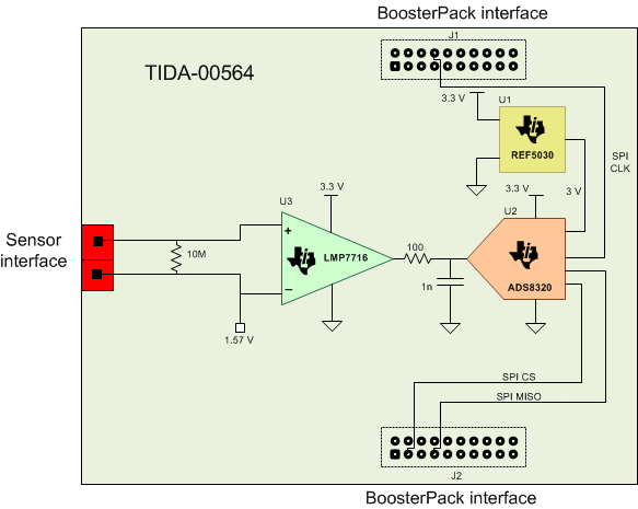 Figure 22. Block Diagram for Universal Sensor IF SAR Booster Pack
8.2.1.1 Design Requirements
This TI Design is a universal sensor IF based on a successive approximation register (SAR) ADC built in a Booster Pack form factor to be easily connected to TI LaunchPad for development and testing. The analog front end (AFE) of the board has been designed for sensors with low output voltage range and high output impedance such as thermopiles, infrared (IR) thermometers, thermocouple amplifiers, pH electrode buffers, piezoelectric accelerometers, and many others.
This application circuit for ADS8320 is designed to achieve the key specifications:
- 16-bit 100 KHz
- Low-input referred noise and low-input bias (100 fA)
- Ideal choice for high-impedance output sensors
8.2.1.2 Detailed Design Procedure
The ADS8320 was selected in this design because it best matches the design’s input requirements and high performance. The maximum throughput rate of the ADS8320 is 100 ksps, the resolution is equal to 16 bits, and the input range of the ADS8320 is equal to the reference voltage supplied to the converter. In this design, the reference voltage is equal to 3 V. The REF5030 features low noise, very low drift, and high initial accuracy for high-performance data converters. The output of the REF5030 is 3 V, which fixes the voltage range of the ADC and can provide a stable reference voltage to maintain the accuracy.
Because the system is targeted for high-impedance output sensors, CMOS or JFET input amplifiers are preferable. The LMP7716 is a CMOS amplifier with low-input referred noise and low-input bias current, which make it an ideal choice for sensor interfaces such as thermopiles, IR thermometers, thermocouple amplifiers, and pH electrode buffers. To ensure the amplifier settles in enough time for the ADC to complete the signal acquisition. The gain bandwidth product of the amplifier is high enough to make sure that the input signal bandwidth is accounted for, and the amplifier is stable with the filter load. The amplifier has a fast slew rate to charge the filter changes and to quickly react to changes of the input.
A low-pass filter must be placed between the input of the ADC and input amplifier. Choosing the capacitor and resistor values play an important role to have a good AFE design. CFLT serves two purposes. Firstly, this capacitor stores energy to charge the ADC internal sampling capacitor. Secondly, CFLT provides a place for the internal capacitor’s charge to go. Due to the storage capabilities of CFLT, this design guide sometimes refers to this capacitor as the flywheel capacitor. CFLT has this alternative name because, like a flywheel, it stores energy for the acquisition time of the ADC. Another name used to describe CFLT is charge reservoir. This TI design has a CFLT equal to 1 nF. This capacitor must be a high-quality capacitor with low voltage and frequency coefficients. The recommended capacitor type is C0G. As a check, make sure the filter capacitor value chosen is at least 20 times the internal capacitor value of ADC. In this case, the value is more than 20 times the size.
The external RFLT | CFLT in the low-pass filter must settle within the ADC acquisition time. As a rule of thumb, set the external RFLT | CFLT settling time constant a bit faster than ideal (for example, 60%) to allow a margin for error of the op-amp load transient and the small signal settling time. TI design has an RFLT equal to 100 Ω. The detailed discussion and calculation can be found in Universal Sensor IF SAR BoosterPack (TIDUAI7).
8.2.1.3 Application Curves
8.2.1.3.1 Static Test (DC)
Figure 23 shows the error, which is the measured output voltage minus the ideal output voltage.
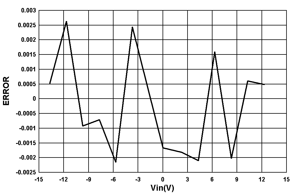 Figure 23. Error (Measured VOUT Minus Ideal VOUT) vs Input Voltage
8.2.1.3.2 Dynamic Test (AC)
For the dynamic test, sine wave is applied at the input of the board with fixed amplitude equal to –1 dBFS and a varying frequency of 0.5 kHz, 1 kHz, 5 kHz, and 10 kHz. Figure 24 shows the test result for 0.5 kHz.
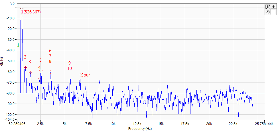 Figure 24. FFT at 500 Hz (Input Signal –1 dBFS)
 |
For step-by-step design procedure, circuit schematics, bill of materials, printed circuit board (PCB) files, simulation results, and test results, refer to TI Precision Design TIDA-00564, Universal Sensor IF SAR Booster Pack Reference Design. |
8.2.2 Wireless Motor Monitor (WMM)
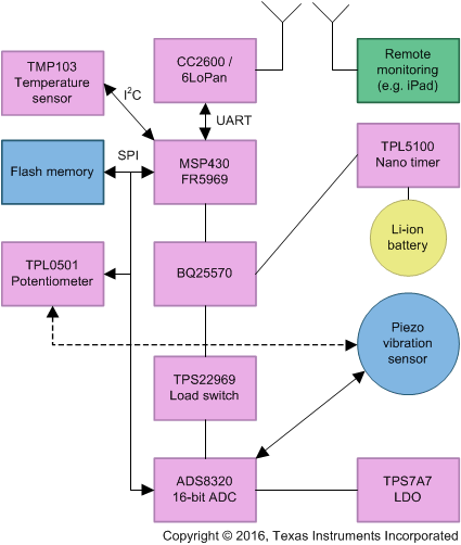 Figure 25. System Block Diagram for Wireless Motor Monitor (WMM)
8.2.2.1 Design Requirements
This application circuit for ADS8320 is designed to achieve the key specifications:
- 16-bit 100 KHz
- 4-K FFT for vibration spectral
- Optimized for ultra-low sleep-mode current: IQ < 45-nA (typical; BQ-harvester in smart mode)
8.2.2.2 Detailed Design Procedure
This TI Design is inspired by the need to monitor the health of motors and machines to accurately predict and schedule maintenance (or replacement) while minimizing cost and down time during industrial production.
This design uses a Piezo vibration sensor to monitor machine vibrations, and a 16-bit precision SAR ADC, ADS8320, is connected to the Piezo shock sensor signal chain for signal acquisition. Because Piezo sensors have high-impedance output nodes, so it’s important to carefully design the analog front-end (AFE) circuitry to reduce the noise and increase the sensitivity of the system, also drive ADS8320 and settle the signal properly during the acquisition time.
8.2.2.3 Application Curves
When testing the system with a portable speaker, the test result graph with 4-K FFT is shown in Figure 26.
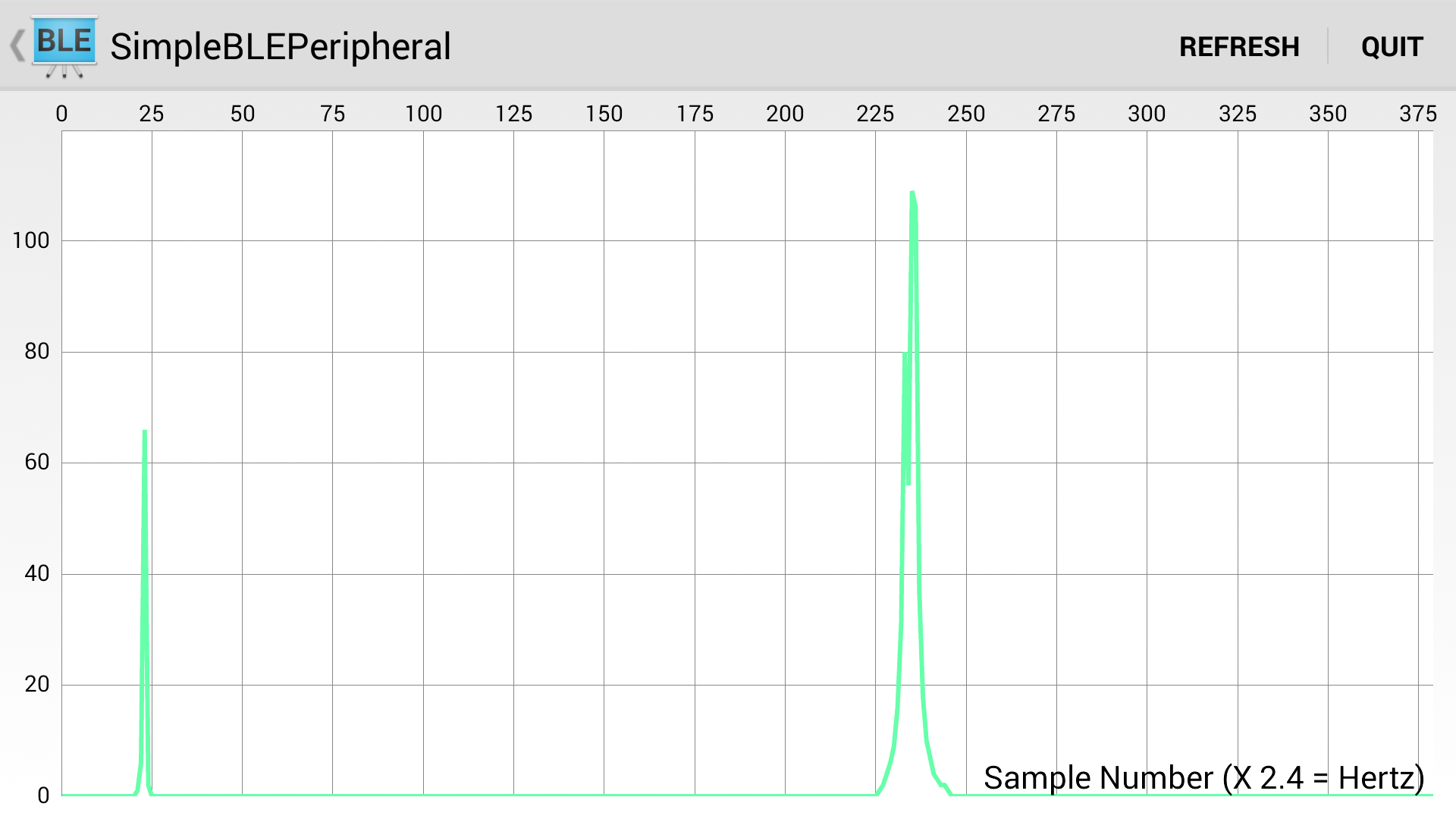 Figure 26. Android Screen Shot of FFT at 600-Hz Excitation With Portable Speaker
When testing the system with a shaker calibrated with a accelerometer, the ADC is used and the AFE gain is set to 11, then configure the software to output 0.1-g of vibration at 500 KHz (or 1.5 KHz, and 2.5 KHz) as depicted in Figure 27.
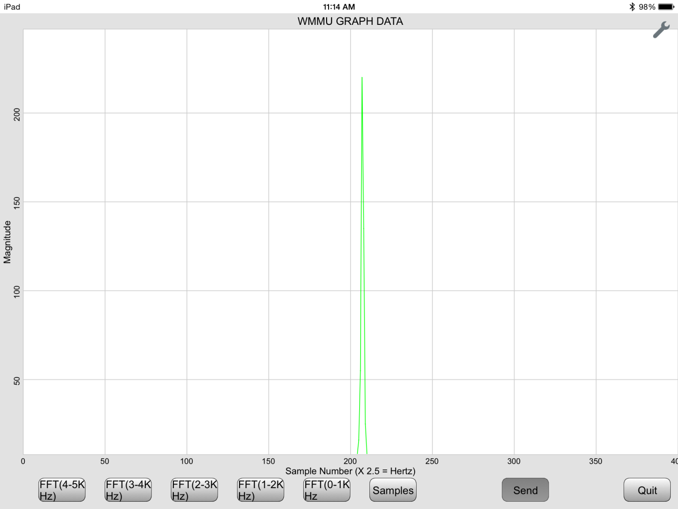 Figure 27. BLE Received FFT at 500-Hz 0.1-g Excitation (X 2.4 = Hertz)
 |
For step-by-step design procedure, circuit schematics, bill of materials, printed circuit board (PCB) files, simulation results, and test results, refer to TI Precision Design TIDM-WLMOTORMONITOR, Wireless Motor Monitor Reference Design. |