SBAS654G June 2014 – January 2020
PRODUCTION DATA.
- 1 Features
- 2 Applications
- 3 Description
- 4 Revision History
- 5 Device Comparison Table
- 6 Pin Configuration and Functions
-
7 Specifications
- 7.1 Absolute Maximum Ratings
- 7.2 ESD Ratings
- 7.3 Recommended Operating Conditions
- 7.4 Thermal Information
- 7.5 Power Ratings
- 7.6 Insulation Specifications
- 7.7 Safety-Related Certifications
- 7.8 Safety Limiting Values
- 7.9 Electrical Characteristics: AMC1305M05
- 7.10 Electrical Characteristics: AMC1305x25
- 7.11 Switching Characteristics
- 7.12 Insulation Characteristics Curves
- 7.13 Typical Characteristics
- 8 Detailed Description
- 9 Application and Implementation
- 10Power Supply Recommendations
- 11Layout
- 12Device and Documentation Support
- 13Mechanical, Packaging, and Orderable Information
7.11 Switching Characteristics
over operating free-air temperature range (unless otherwise noted)| PARAMETER | MIN | TYP | MAX | UNIT | |
|---|---|---|---|---|---|
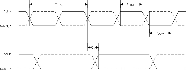
| tCLK | CLKIN, CLKIN_N clock period | 49.75 | 50 | 200 | ns |
| tHIGH | CLKIN, CLKIN_N clock high time | 19.9 | 25 | 120 | ns |
| tLOW | CLKIN, CLKIN_N clock low time | 19.9 | 25 | 120 | ns |
| tD | Falling edge of CLKIN, CLKIN_N to DOUT, DOUT_N valid delay,
CLOAD = 5 pF |
0 | 15 | ns | |
| tISTART | Interface startup time
(DVDD at 3.0 V min to DOUT, DOUT_N valid with AVDD ≥ 4.5 V) |
32 | 32 | CLKIN cycles | |
| tASTART | Analog startup time (AVDD step up to 4.5 V with DVDD ≥ 3.0 V) | 1 | ms | ||
 Figure 1. Digital Interface Timing
  Figure 2. Digital Interface Startup Timing