SBAS655F September   2014  – January 2020

PRODUCTION DATA.  

  1. Features
  2. Applications
  3. Description
    1.     Device Images
      1.      Simplified Schematic
  4. Revision History
  5. Device Comparison Table
  6. Pin Configuration and Functions
    1.     Pin Functions
  7. Specifications
    1. 7.1  Absolute Maximum Ratings
    2. 7.2  ESD Ratings
    3. 7.3  Recommended Operating Conditions
    4. 7.4  Thermal Information
    5. 7.5  Power Ratings
    6. 7.6  Insulation Specifications
    7. 7.7  Safety-Related Certifications
    8. 7.8  Safety Limiting Values
    9. 7.9  Electrical Characteristics: AMC1304x05
    10. 7.10 Electrical Characteristics: AMC1304x25
    11. 7.11 Switching Characteristics
    12. 7.12 Insulation Characteristics Curves
    13. 7.13 Typical Characteristics
  8. Detailed Description
    1. 8.1 Overview
    2. 8.2 Functional Block Diagram
    3. 8.3 Feature Description
      1. 8.3.1 Analog Input
      2. 8.3.2 Modulator
      3. 8.3.3 Digital Output
    4. 8.4 Device Functional Modes
      1. 8.4.1 Fail-Safe Output
      2. 8.4.2 Output Behavior in Case of a Full-Scale Input
  9. Application and Implementation
    1. 9.1 Application Information
      1. 9.1.1 Digital Filter Usage
    2. 9.2 Typical Applications
      1. 9.2.1 Frequency Inverter Application
        1. 9.2.1.1 Design Requirements
        2. 9.2.1.2 Detailed Design Procedure
        3. 9.2.1.3 Application Curve
      2. 9.2.2 Isolated Voltage Sensing
        1. 9.2.2.1 Design Requirements
        2. 9.2.2.2 Detailed Design Procedure
        3. 9.2.2.3 Application Curve
      3. 9.2.3 What To Do and What Not To Do
  10. 10Power Supply Recommendations
  11. 11Layout
    1. 11.1 Layout Guidelines
    2. 11.2 Layout Examples
  12. 12Device and Documentation Support
    1. 12.1 Device Support
      1. 12.1.1 Device Nomenclature
    2. 12.2 Documentation Support
      1. 12.2.1 Related Documentation
    3. 12.3 Related Links
    4. 12.4 Receiving Notification of Documentation Updates
    5. 12.5 Community Resources
    6. 12.6 Trademarks
    7. 12.7 Electrostatic Discharge Caution
    8. 12.8 Glossary
  13. 13Mechanical, Packaging, and Orderable Information

Application Curve

In motor control applications, a very fast response time for overcurrent detection is required. The time for fully settling the filter in case of a step-signal at the input of the modulator depends on its order; that is, a sinc3 filter requires three data updates for full settling (with fDATA = fCLK / OSR). Therefore, for overcurrent protection, filter types other than sinc3 can be a better choice; an alternative is the sinc2 filter. Figure 55 compares the settling times of different filter orders.

The delay time of the sinc filter with a continuous signal is half of its settling time.
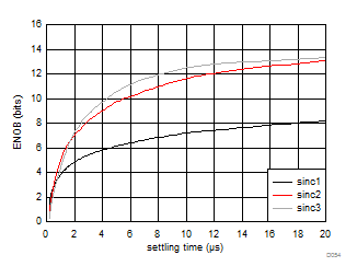
AMC1304L05 AMC1304L25 AMC1304M05 AMC1304M25 D054_SBAS654.gif
Figure 55. Measured Effective Number of Bits versus Settling Time