SBAS655F September 2014 – January 2020
PRODUCTION DATA.
- 1 Features
- 2 Applications
- 3 Description
- 4 Revision History
- 5 Device Comparison Table
- 6 Pin Configuration and Functions
-
7 Specifications
- 7.1 Absolute Maximum Ratings
- 7.2 ESD Ratings
- 7.3 Recommended Operating Conditions
- 7.4 Thermal Information
- 7.5 Power Ratings
- 7.6 Insulation Specifications
- 7.7 Safety-Related Certifications
- 7.8 Safety Limiting Values
- 7.9 Electrical Characteristics: AMC1304x05
- 7.10 Electrical Characteristics: AMC1304x25
- 7.11 Switching Characteristics
- 7.12 Insulation Characteristics Curves
- 7.13 Typical Characteristics
- 8 Detailed Description
- 9 Application and Implementation
- 10Power Supply Recommendations
- 11Layout
- 12Device and Documentation Support
- 13Mechanical, Packaging, and Orderable Information
8.3.2 Modulator
The modulator implemented in the AMC1304 is a second-order, switched-capacitor, feed-forward ΔΣ modulator, such as the one conceptualized in Figure 48. The analog input voltage VIN and the output V5 of the 1-bit digital-to-analog converter (DAC) are differentiated, providing an analog voltage V1 at the input of the first integrator stage. The output of the first integrator feeds the input of the second integrator stage, resulting in output voltage V3 that is differentiated with the input signal VIN and the output of the first integrator V2. Depending on the polarity of the resulting voltage V4, the output of the comparator is changed. In this case, the 1-bit DAC responds on the next clock pulse by changing its analog output voltage V5, causing the integrators to progress in the opposite direction and forcing the value of the integrator output to track the average value of the input.
 Figure 48. Block Diagram of a Second-Order Modulator
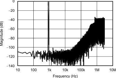
 The modulator shifts the quantization noise to high frequencies, as shown in Figure 49. Therefore, use a low-pass digital filter at the output of the device to increase the overall performance. This filter is also used to convert from the 1-bit data stream at a high sampling rate into a higher-bit data word at a lower rate (decimation). TI's microcontroller families TMS320F2807x and TMS320F2837x offer a suitable programmable, hardwired filter structure termed a sigma-delta filter module (SDFM) optimized for usage with the AMC1304 family. Also, SD24_B converters on the MSP430F677x microcontrollers offer a path to directly access the integrated sinc-filters, thus offering a system-level solution for multichannel, isolated current sensing. An additional option is to use a suitable application-specific device, such as the AMC1210 (a four-channel digital sinc-filter). Alternatively, a field-programmable gate array (FPGA) can be used to implement the digital filter.
