SBAS655F September 2014 – January 2020
PRODUCTION DATA.
- 1 Features
- 2 Applications
- 3 Description
- 4 Revision History
- 5 Device Comparison Table
- 6 Pin Configuration and Functions
-
7 Specifications
- 7.1 Absolute Maximum Ratings
- 7.2 ESD Ratings
- 7.3 Recommended Operating Conditions
- 7.4 Thermal Information
- 7.5 Power Ratings
- 7.6 Insulation Specifications
- 7.7 Safety-Related Certifications
- 7.8 Safety Limiting Values
- 7.9 Electrical Characteristics: AMC1304x05
- 7.10 Electrical Characteristics: AMC1304x25
- 7.11 Switching Characteristics
- 7.12 Insulation Characteristics Curves
- 7.13 Typical Characteristics
- 8 Detailed Description
- 9 Application and Implementation
- 10Power Supply Recommendations
- 11Layout
- 12Device and Documentation Support
- 13Mechanical, Packaging, and Orderable Information
10 Power Supply Recommendations
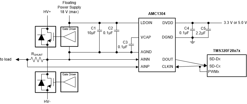
In a typical frequency-inverter application, the high-side power supply (LDOIN) for the device is directly derived from the floating power supply of the upper gate driver. A low-ESR decoupling capacitor of 0.1 µF is recommended for filtering this power-supply path. Place this capacitor (C2 in Figure 58) as close as possible to the LDOIN pin of the AMC1304 for best performance. If better filtering is required, an additional 10-µF capacitor can be used. The output of the internal LDO requires a decoupling capacitor of 0.1 µF to be connected between the VCAP pin and AGND as close as possible to the device.
The floating ground reference (AGND) is derived from the end of the shunt resistor, which is connected to the negative input (AINN) of the device. If a four-pin shunt is used, the device inputs are connected to the inner leads and AGND is connected to one of the outer leads of the shunt.
For decoupling of the digital power supply on the controller side, TI recommends using a 0.1-µF capacitor assembled as close to the DVDD pin of the AMC1304 as possible, followed by an additional capacitor in the range of 1 µF to 10 µF.
