SBAU171D May   2010  – January 2016 ADS1198 , ADS1298


  1.   ADS1298ECG-FE/ADS1198ECG-FE
    1.     Trademarks
    2. 1 ADS1298ECG-FE/ADS1198ECG-FE Overview
      1. 1.1 Important Disclaimer Information
      2. 1.2 Introduction
      3. 1.3 Supported Features
      4. 1.4 Features Not Supported in Current Version
      5. 1.5 ADS1x98ECG-FE Hardware
      6. 1.6 Minimum System Requirements for ADS1x98ECG-FE Evaluation Software
    3. 2 Quick Start
      1. 2.1 Default Jumper/Switch Configuration
      2. 2.2 ADS1x98ECG-FE Operation
    4. 3 Using the ADS1298ECG-FE Software
      1. 3.1 Application User Menu
      2. 3.2 Top-Level Application Controls
      3. 3.3 About Tab
      4. 3.4 ADC Register Tab
        1. 3.4.1 Standby and Reset Controls
        2. 3.4.2 Channel Registers Tab (ADC Register)
          1. 3.4.2.1 Global Channel Registers
          2. 3.4.2.2 Channel Control Registers
        3. 3.4.3 LOFF and RLD Tab (ADC Register)
          1. 3.4.3.1 Lead-Off Detection and Current Direction Control Registers
          2. 3.4.3.2 Right Leg Drive Derivation Control Registers
        4. 3.4.4 GPIO and OTHER Registers Tab (ADC Register)
          1. 3.4.4.1 Wilson Central and Augmented Lead Registers
        5. 3.4.5 Register Map (ADC Register)
      5. 3.5 Analysis Tab
        1. 3.5.1 Scope Tab (Anaysis)
          1. 3.5.1.1 Zoom Tool
        2. 3.5.2 Histogram Tab (Analysis)
        3. 3.5.3 FFT Tab
        4. 3.5.4 ECG Tab (Analysis)
      6. 3.6 Save Tab
    5. 4 ADS1x98ECG-FE Input Signals
      1. 4.1 Input Short Testing
      2. 4.2 Internal Test Signals Input
      3. 4.3 Temperature Sensor
      4. 4.4 Normal Electrode Input
        1. 4.4.1 Capturing 12-Lead ECG Signals
      5. 4.5 MVDD Input, RLD Measurement, RLD Positive Electrode Driver, and RLD Negative Electrode Driver
      6. 4.6 Lead Derivation
      7. 4.7 Wilson Center Terminal (WCT)
      8. 4.8 Right Leg Drive
        1. 4.8.1 RLD Common Mode Voltage
        2. 4.8.2 Driving the RLD Cable Shield
      9. 4.9 PACE Detection
    6. 5 ADS1298ECG-FE/ADS1198ECG-FE Hardware Details
      1. 5.1 Jumper Description
      2. 5.2 Power Supply
      3. 5.3 Clock
      4. 5.4 Reference
      5. 5.5 Analog Output Signals
      6. 5.6 Digital Signals
      7. 5.7 Analog Input Signals
        1. 5.7.1 Patient Simulator Input
        2. 5.7.2 Arbitrary Input Signals
  2. ASchematics, BOM, Layout, and ECG Cable Details
    1. A.1 Overview
    2. A.2 ADS1x98ECG-FE Front-End Board Schematics
    3. A.3 Bill of Materials
      1. Table 13. Bill of Materials: ADS1x98ECG-FE
    4. A.4 Printed Circuit Board Layout
    5. A.5 ECG Cable Details
  3. BExternal Optional Hardware
    1. B.1 Optional External Hardware (Not Included)
    2. B.2 ADS1x98ECG-FE Power-Supply Recommendations
  4. CSoftware Installation
    1. C.1 Minimum Requirements
    2. C.2 Installing the Software

Global Channel Registers

The Global Channel Registers box includes Configuration Register 1 (CONFIG1), Configuration Register 2 (CONFIG2), Configuration Register 3 (CONFIG3), and Lead Off Control Register (LOFF). The upper half of Figure 8 shows the section of the UI panel that allows manipulation and control of these registers.

Configuration Register 1 enables the user to control the resolution mode, enable the daisy-chain configuration options, and program the data rate.

NOTE

Since the HR bit is not available in the ADS1198, the Configuration Register 1 control will not show this control when testing the ADS1198.

Configuration Register 2 enables the user to select an internal square wave test source amplitude of ±1mV or ±2mV and a frequency of DC, 2Hz (fCLK/221), or 4Hz (fCLK/220).

Configuration Register 3 controls the bandgap reference (illustrated in Figure 9) and right leg drive (RLD) options. This register enables the user to select between an external or internal reference voltage, enable/disable the internal reference buffer, toggle between a 2.4V or a 4.0V output voltage, and to enable/disable the RLD as well as choose whether the RLD voltage is provided internally or externally.
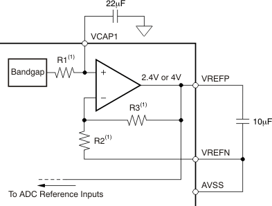
ai_internal_ref_buff_conn_bau171.gifFigure 9. Internal Reference and Buffer Connections

The Lead-Off Control Register allows the user to configure the threshold for the lead-off comparator, resistive pull-up or current-source excitation, the lead-off current magnitude, and DC or AC detection. Figure 10 illustrates a simplified diagram of the resistive pull-up and excitation options for the lead-off detect feature.
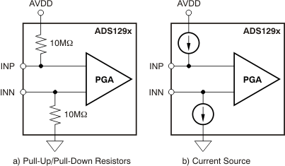
ai_dc_leadoff_bau171.gifFigure 10. Lead-Off Excitation Options