SBAU321B November   2018  – June 2021 ADS7142 , ADS7142-Q1


  1.   Trademarks
  2. 1Introduction
  3. 2BOOSTXL-ADS7142-Q1 EVM Overview
    1. 2.1 Connectors for Single-Ended Analog Input
    2. 2.2 Digital Interface
    3. 2.3 ADS7142-Q1 Digital I/O Interface
    4. 2.4 Power Supplies
  4. 3BOOSTXL-ADS7142-Q1 EVM Initial Setup
    1. 3.1 Running ADS7142-Q1 GUI Online and TI Cloud Agent Application Installation
    2. 3.2 Hardware Setup Instructions
    3. 3.3 ADS7142-Q1 GUI Description
      1. 3.3.1 Description
      2. 3.3.2 REGMAP
      3. 3.3.3 Functional Mode
      4. 3.3.4 General Instructions
  5. 4ADS7142-Q1 GUI Functional Modes
    1. 4.1 Autonomous Mode
      1. 4.1.1 Start Burst Mode
      2. 4.1.2 Stop Burst Mode
      3. 4.1.3 Pre Alert Mode
      4. 4.1.4 Post Alert Mode
    2. 4.2 High Precision Mode
    3. 4.3 Manual Mode
      1. 4.3.1 Default Mode
      2. 4.3.2 Auto Mode
    4. 4.4 Temperature Monitoring Using BOOSTXL-ADS7142-Q1
    5. 4.5 Input Signal Conditioning Block on the BOOSTXL-ADS7142-Q1
  6. 5Bill of Materials, Printed-Circuit Board Layout, and Schematics
    1. 5.1 Bill of Materials
    2. 5.2 PCB Layout
    3. 5.3 Schematics
  7. 6Revision History

REGMAP

Figure 3-4 shows register map page for the ADS7142-Q1. On the top right corner, options to read registers individually, read all the registers at once, or write individual register are available. Users can choose to have the register values modified in the GUI to be written on the device instantaneously by selecting the Immediate option or later using the Deferred option.
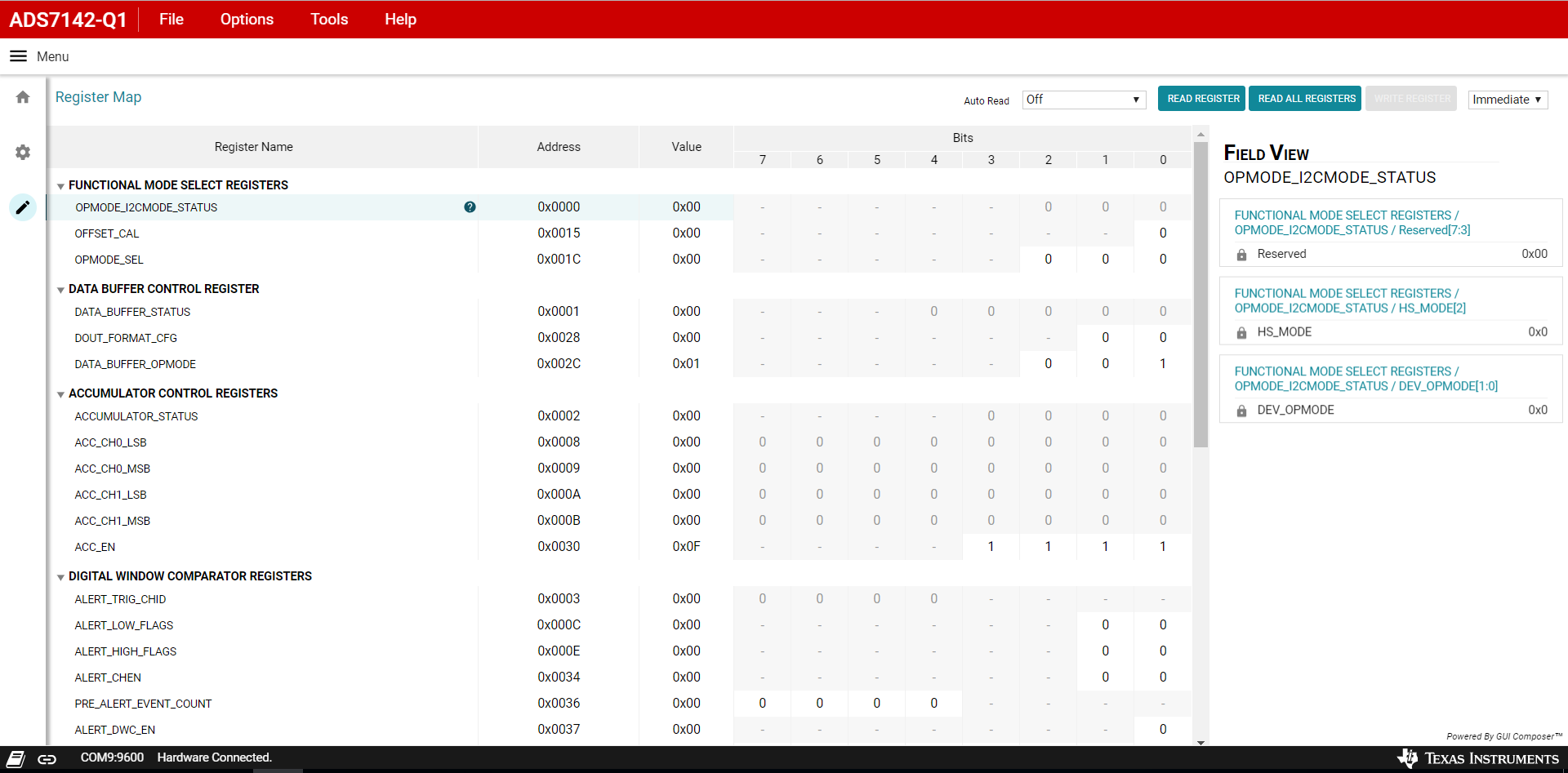
GUID-5D7703D7-32FB-454C-8B66-BD0B1866FC02-low.pngFigure 3-4 ADS7142-Q1 Register Map Page