SBAU352 June 2020 ADS131B04-Q1
2.1 ADC Analog Input Signal Path
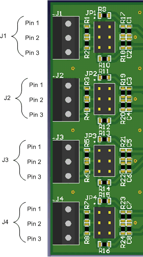
Analog inputs to the EVM can be connected to either the terminal blocks or to the header pins associated with each ADC channel. The 3x2 100-mil headers for each channel allow the user to configure the inputs differentially depending on the signal to be measured. The screw terminal blocks can interface directly with the leads of an external sensor input. Figure 2 shows the signal chain used for all four input channels on the EVM and is used to describe the supported input options in Figure 3, Table 2, and Table 3.
External voltage inputs can be applied to J1 pins 1 and 3. For single-ended inputs, install a jumper on either JP1[1-2] or JP1[5-6] to connect an input to the EVM ground. If the external voltage is applied through a series resistor, R1 or R2 can be used to form a resistor divider by installing JP1[3-4] to support higher voltage measurements. Input jumper connections are described in Table 2. Similarly, R17 and R18 can be installed to form a resistor divider with the series 49.9-Ω resistors on each input. An input must not be applied such that the voltage on the input pins of the ADS131B04-Q1 exceeds the absolute maximum ratings. For more details, see the ADS131B04-Q1 data sheet.
R1 and R2 also present a 2-kΩ differential load when all jumpers on JP1 are uninstalled. This load acts as a burden resistor for a current transformer (CT) input. For single-ended measurements, the unused end of the transformer secondary side can be tied to ground by installing the appropriate jumper on JP1.
R9, R10, and C9 form a differential low-pass filter with a –3-dB cutoff frequency of 1.594 MHz. The series impedance is kept relatively low in order to maintain adequate total harmonic distortion (THD) performance.
 Figure 2. Input Terminal Blocks and Headers (Schematic)
  Figure 3. Input Terminal Blocks and Headers (PCB)
 Table 2. Analog Input Terminal Blocks, J1–J4
| Terminal Block | Pin | Function | ADS131B04-Q1 Input Pin |
|---|---|---|---|
| J1 | 1 | Channel 0 positive input | AIN0P |
| 2 | EVM ground | AGND and DGND | |
| 3 | Channel 0 negative input | AIN0N | |
| J2 | 1 | Channel 1 positive input | AIN1P |
| 2 | EVM ground | AGND and DGND | |
| 3 | Channel 1 negative input | AIN1N | |
| J3 | 1 | Channel 2 positive input | AIN2P |
| 2 | EVM ground | AGND and DGND | |
| 3 | Channel 2 negative input | AIN2N | |
| J4 | 1 | Channel 3 positive input | AIN3P |
| 2 | EVM ground | AGND and DGND | |
| 3 | Channel 3 negative input | AIN3N |
Table 3. Analog Input Jumper Connection, JP1–JP4
| Jumper | Position | Description |
|---|---|---|
| JP1 | Connection for channel 0 analog inputs | |
| [1-2] | Short positive input to ground | |
| [3-4] | Connect both inputs to ground via 1-kΩ resistors (default) | |
| [5-6] | Short negative input to ground | |
| JP2 | Connection for channel 1 analog inputs | |
| [1-2] | Short positive input to ground | |
| [3-4] | Connect both inputs to ground via 1-kΩ resistors (default) | |
| [5-6] | Short negative input to ground | |
| JP3 | Connection for channel 2 analog inputs | |
| [1-2] | Short positive input to ground | |
| [3-4] | Connect both inputs to ground via 1-kΩ resistors (default) | |
| [5-6] | Short negative input to ground | |
| JP4 | Connection for channel 3 analog inputs | |
| [1-2] | Short positive input to ground | |
| [3-4] | Connect both inputs to ground via 1-kΩ resistors (default) | |
| [5-6] | Short negative input to ground | |